kkpcb04 - KKPCB - Page 20 of 104
 
HomeAuthor

kkpcb04 - KKPCB - Page 20 of 104

High Current PCB Design: How to Handle Large Current in Power Electronics

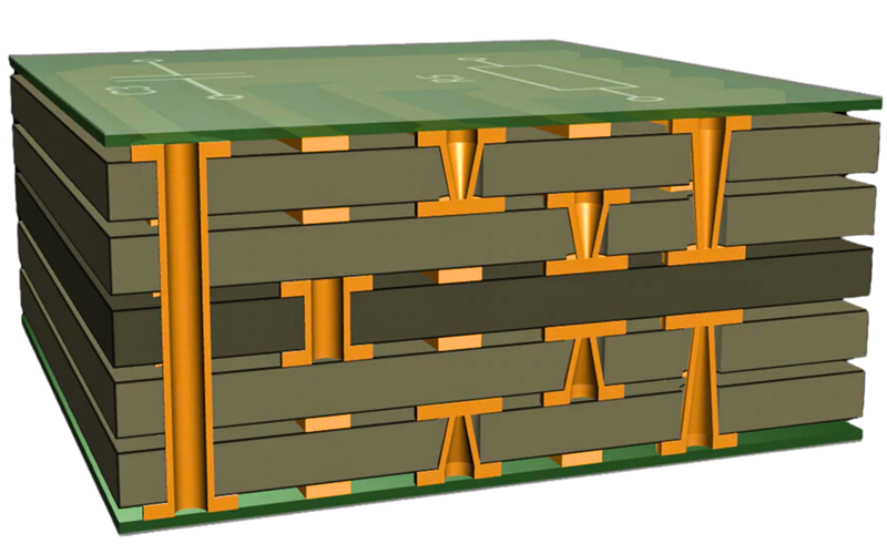
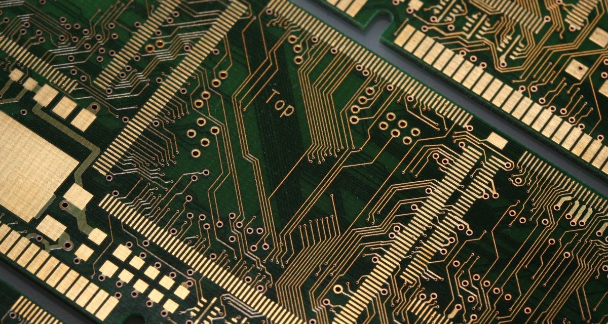
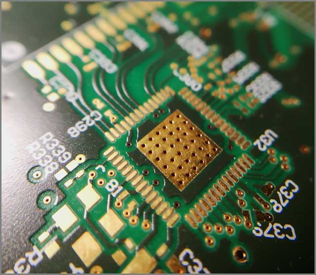
In many modern electronic systems, circuit boards must carry significantly higher currents than standard PCB designs. Applications such as power supplies, motor controllers, battery management systems, and industrial equipment require high current PCBs capable of safely handling large electrical loads. Designing a PCB for high current applications involves more than simply increasing the trace width....

Microvia PCB Technology: Enabling High-Density Interconnect Designs

As electronic products continue to shrink in size while increasing in functionality, traditional PCB technologies face limitations in routing density and signal performance. Microvia PCB technology has emerged as a key solution for supporting high-density interconnect (HDI) designs in modern electronics. By using extremely small vias to connect circuit layers, microvia PCBs allow engineers to...

High Reliability PCB: Key Design Principles for Mission-Critical Electronics

In many industries, electronic systems must operate reliably under extreme conditions. Whether used in aerospace equipment, medical devices, or industrial control systems, circuit boards must deliver consistent performance without failure. This is where high reliability PCBs become essential. Unlike standard circuit boards, high reliability PCBs are specifically engineered to withstand environmental stress, electrical load, and...

Thermal Management PCB: Design Strategies for Efficient Heat Dissipation in Electronics

As electronic devices become more powerful and compact, heat generation inside circuit boards has become a major engineering challenge. Excessive heat can reduce performance, shorten component lifespan, and even lead to system failure. For this reason, thermal management PCB design has become an essential part of modern electronics development. From power electronics and LED lighting...

Why Multilayer PCBs Are Essential for High-Speed and High-Density Electronics

As electronic devices continue to evolve toward higher performance and smaller form factors, traditional two-layer circuit boards are no longer sufficient for many modern applications. This is where multilayer PCBs play a crucial role. By integrating multiple conductive layers into a single compact structure, multilayer PCBs enable engineers to design complex circuits while maintaining signal...

Low Loss PCB for High-Frequency and High-Speed Signal Applications

As modern electronic systems operate at increasingly higher frequencies and faster data rates, signal loss has become a major challenge in PCB design. Low Loss PCBs are specifically engineered to minimize signal attenuation and maintain signal integrity in high-speed and high-frequency circuits. Unlike conventional FR-4 boards, low loss PCBs use advanced dielectric materials with lower...

ATE PCB Assembly for High-Performance Automated Test Equipment

Introduction to ATE PCB Assembly ATE PCB Assembly refers to the manufacturing and integration of printed circuit boards used in Automated Test Equipment (ATE) systems. These boards are specifically designed to support the testing of semiconductor devices, integrated circuits, and electronic components with high precision and reliability. Because ATE systems operate in demanding test environments,...

Custom ATE PCB Design for Reliable Semiconductor Testing

Custom ATE PCB Automated Test Equipment (ATE) plays a critical role in modern electronics manufacturing, ensuring that integrated circuits, semiconductor devices, and electronic assemblies perform according to specification. At the heart of this process is the What Is a Custom ATE PCB? A Custom ATE PCB is a dedicated testing interface board designed to connect...

Multilayer Test PCB: Design, Manufacturing, and Applications

A Multilayer Test PCB is a specialized printed circuit board designed for testing, validation, and performance verification of electronic components, integrated circuits, and complex systems. Compared with standard PCBs, multilayer test boards incorporate multiple conductive layers to support high-density routing, signal integrity analysis, and accurate electrical testing. With the rapid development of modern electronics such...

HDI PCB: Design, Microvia Technology, and High-Density Applications

High Density Interconnect (HDI) PCB technology is designed to support modern electronic devices that demand higher performance, smaller form factors, and greater circuit complexity. HDI PCBs use advanced manufacturing techniques such as microvias, blind vias, buried vias, and fine line routing to increase the wiring density compared to traditional multilayer PCBs. As electronic products continue...