signal integrity PCB - KKPCB
 
HomeTag

signal integrity PCB - KKPCB

Controlled Impedance PCB Prototype: Reducing Risk in High-Speed and RF Design Validation

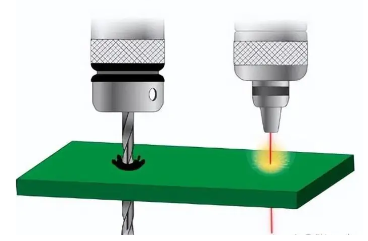
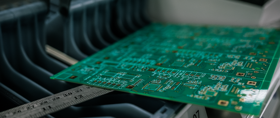
For high-speed digital and RF electronic systems, signal integrity is one of the most critical design challenges. A controlled impedance PCB prototype plays a key role in validating design assumptions, manufacturing tolerances, and electrical performance before moving into mass production. Building controlled impedance into the prototype stage significantly reduces technical and production risk. What Is...

Controlled Impedance PCB Prototype: Accurate Signal Integrity Validation from Design to Production

As data rates and operating frequencies continue to increase, maintaining signal integrity becomes a critical design challenge. A controlled impedance PCB prototype allows engineers to verify impedance accuracy, minimize signal reflection, and validate high-speed or RF performance before entering mass production. By prototyping controlled impedance PCBs early, design risks are reduced and product reliability is...

Controlled Impedance PCB Prototype: Precision Prototyping for High-Speed and RF Designs

As data rates and operating frequencies continue to increase, signal integrity becomes a critical factor even at the prototype stage. A controlled impedance PCB prototype allows engineers to validate high-speed and RF signal performance before entering volume production. Accurate impedance control during PCB prototyping helps reduce reflections, minimize signal loss, and ensure design reliability from...

Controlled Impedance PCB Prototype: Ensuring Signal Integrity in High-Speed and RF Designs

As digital speeds and operating frequencies continue to increase, maintaining signal integrity has become one of the biggest challenges in PCB design. A controlled impedance PCB prototype is a critical step in validating transmission line performance before mass production. By accurately controlling impedance during prototyping, engineers can reduce signal reflection, minimize loss, and ensure stable...

Designing Buried Via PCBs for High-Density Routing and Signal Integrity Optimization

As electronic systems continue to evolve toward higher speeds, smaller form factors, and increased functionality, traditional through-hole via structures are becoming a limiting factor. Buried Via PCB technology has emerged as a key solution for achieving high-density routing and optimizing signal integrity, especially in HDI, high-speed digital, and RF designs. By embedding vias between internal...

Designing High Layer Count PCBs for Complex Signal, Power, and Thermal Integrity Challenges

As electronic systems continue to integrate higher data rates, greater power density, and tighter form factors, high layer count PCBs have become a foundational platform for modern hardware architecture. Designs exceeding 16, 20, or even 30 layers are now common in data center equipment, telecommunications infrastructure, aerospace electronics, and industrial control systems. However, increasing layer...

Controlled Impedance PCB Engineering for High-Speed Digital and High-Frequency RF Applications

A Controlled Impedance PCB is a critical foundation for modern high-speed digital systems and high-frequency RF applications. As signal rise times shrink and operating frequencies extend into multi-GHz ranges, PCB interconnects must behave as predictable transmission lines rather than simple copper connections. Controlled Impedance PCB design ensures signal integrity, phase stability, and EMI compliance across...

Enable Ultra-High Interconnect Density and Signal Integrity with Advanced High Layer Count PCB Architectures

High Layer Count PCB: The Backbone of Complex Electronic Systems A High Layer Count PCB refers to a multilayer printed circuit board typically featuring 16 layers, 24 layers, 32 layers, or more, designed to support complex signal routing, dense interconnections, and advanced power distribution. As electronic systems continue to integrate higher data rates, tighter form...

Enhance Routing Density and Signal Integrity with Buried Via PCB Architectures for High-Density Electronic Systems

Buried Via PCB: Enabling High-Density Interconnection Beyond Conventional Multilayer Boards A Buried Via PCB is a multilayer printed circuit board in which vias connect only internal layers and do not extend to the outer layers. Unlike through-hole vias, buried vias are completely embedded within the PCB stackup, enabling higher routing density, improved signal integrity, and...

Enable Ultra-Complex Routing and Signal Integrity with High Layer Count PCB Architectures for Advanced Electronic Systems

High Layer Count PCB: The Backbone of Ultra-Complex Electronic Integration A High Layer Count PCB refers to a multilayer printed circuit board typically exceeding 12 layers and extending to 20, 30, or even 60+ layers for advanced electronic systems. High layer count PCB designs are essential for applications requiring dense routing, high-speed signal transmission, controlled...