Sequential Lamination PCB - KKPCB
 
HomeTag

Sequential Lamination PCB - KKPCB

Buried Via PCB – Advanced Multilayer PCB Technology for High-Density Circuit Design

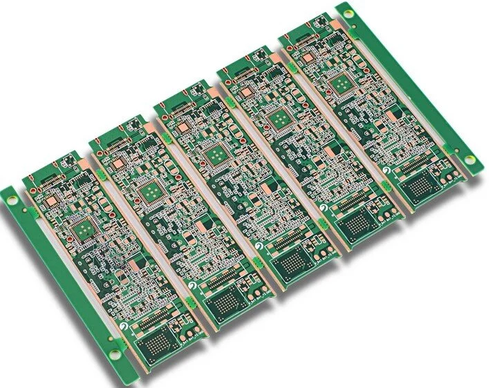
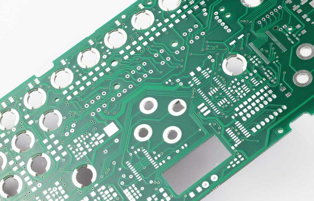
What Is a Buried Via PCB? A Buried Via PCB is a type of multilayer printed circuit board that uses buried vias to connect internal copper layers without reaching the outer surface layers. Unlike through-hole vias that pass through the entire board, buried vias exist only between inner layers, remaining invisible from the exterior of...

HDI PCB – High Density Interconnect PCB for Advanced Electronics

What Is HDI PCB? HDI PCB (High Density Interconnect PCB) is a printed circuit board designed with higher wiring density per unit area compared to traditional multilayer PCBs. It uses advanced manufacturing technologies such as microvias, blind vias, buried vias, and fine line traces to achieve compact size and improved electrical performance. HDI PCB is...

Buried Via PCB – Advanced Multilayer PCB with Internal Interconnection Technology

What Is a Buried Via PCB? A Buried Via PCB is a multilayer printed circuit board that contains vias connecting internal layers only, without reaching the outer surface layers. Unlike through-hole vias, buried vias are completely enclosed within the board stack-up. This allows designers to: Increase routing density Optimize outer layer space Improve signal integrity...

High Layer Count PCB – Advanced Multilayer PCB for High Density and High Speed Applications

What Is a High Layer Count PCB? A High Layer Count PCB refers to a multilayer printed circuit board typically built with 16 layers or more, and in advanced applications, up to 40, 60, or even higher layer counts. High Layer Count PCB is designed to support: High density routing Complex signal distribution Controlled impedance...

From Stackup Planning to Lamination Control: Engineering High Layer Count PCBs That Actually Work

Engineering High Layer Count PCBs: Why “More Layers” Isn’t the Answer As electronic systems evolve toward higher speeds, higher integration, and smaller form factors, high layer count PCBs—typically 16 layers and above—have become standard in data centers, telecommunications, aerospace electronics, and advanced industrial systems. However, many multilayer PCBs fail not because of schematic errors, but...

Enhance Routing Density and Signal Integrity with Buried Via PCB Architectures for High-Density Electronic Systems

Buried Via PCB: Enabling High-Density Interconnection Beyond Conventional Multilayer Boards A Buried Via PCB is a multilayer printed circuit board in which vias connect only internal layers and do not extend to the outer layers. Unlike through-hole vias, buried vias are completely embedded within the PCB stackup, enabling higher routing density, improved signal integrity, and...