semiconductor test PCB - KKPCB
 
HomeTag

semiconductor test PCB - KKPCB

HDI PCB: Advanced High-Density Interconnect Solutions for Compact and High-Speed Electronics

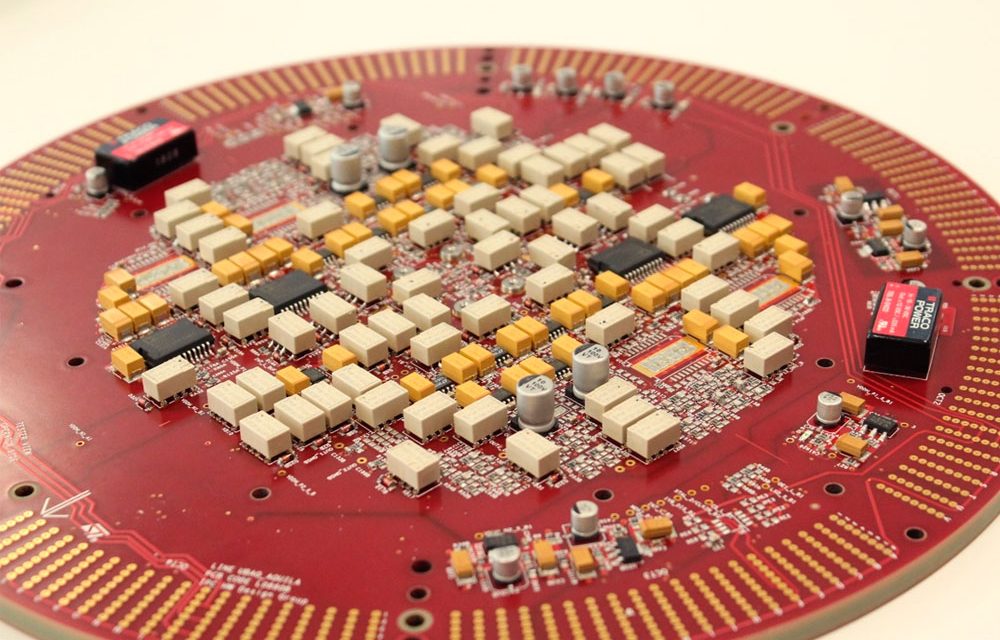
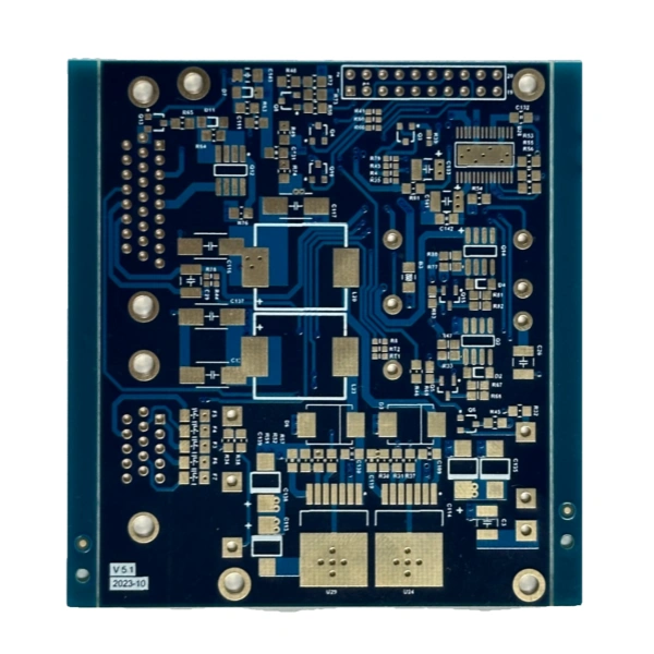
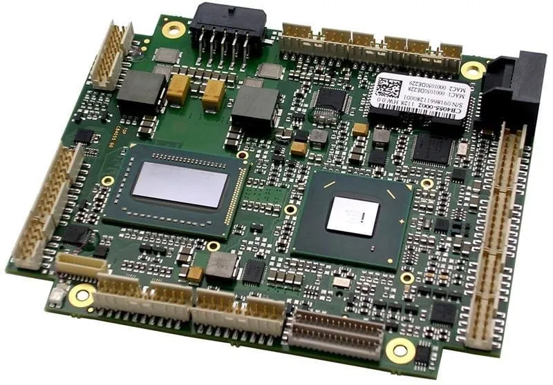
As electronic devices become smaller, faster, and more complex, traditional PCB technologies often struggle to meet space and performance requirements. The HDI PCB (High-Density Interconnect PCB) addresses these challenges by enabling ultra-dense routing, shorter signal paths, and improved electrical performance in compact form factors. A professionally designed HDI PCB is essential for modern high-speed, high-pin-count,...

High Pin Count PCB: Enabling Dense Interconnects for Advanced Semiconductor and High-Speed Systems

As semiconductor devices and high-performance modules continue to scale in complexity, the number of required electrical connections has increased dramatically. The High Pin Count PCB is designed to manage hundreds or even thousands of pins while maintaining signal integrity, mechanical reliability, and manufacturability. A well-designed High Pin Count PCB is critical for advanced computing, communication,...

Test Socket PCB: Designing Stable, Long-Life Interfaces for High-Cycle Semiconductor Testing

In semiconductor mass production, testing does not fail because of the device alone—very often, failures originate from unstable test interfaces. The Test Socket PCB plays a decisive role in ensuring that electrical contact, signal transmission, and mechanical alignment remain consistent across thousands or even millions of test cycles. A professionally designed Test Socket PCB directly...

Load Board PCB: High-Reliability Test Interfaces for High-Volume Semiconductor Production

In semiconductor mass production, test throughput and consistency are just as important as accuracy. The Load Board PCB is a critical interface between automated test equipment (ATE) and packaged semiconductor devices, ensuring reliable electrical connection and repeatable test performance during high-volume production. A well-designed Load Board PCB minimizes downtime, reduces false failures, and supports long-term...

Semiconductor Test PCB: Reliable Test Platforms from Wafer Validation to Final Device Qualification

Semiconductor devices must pass multiple test stages before entering mass production and end-use applications. At every stage, the Semiconductor Test PCB plays a vital role in ensuring accurate measurement, stable operation, and repeatable test results. Whether used in wafer probing, package testing, or final system validation, a well-designed semiconductor test PCB directly impacts yield, reliability,...

Probe Card PCB: Precision Interconnect Solutions for Wafer-Level Semiconductor Testing

Wafer-level testing is one of the most demanding stages in semiconductor manufacturing. At this level, accuracy, repeatability, and mechanical precision are critical. The Probe Card PCB serves as the core platform that connects automated test equipment (ATE) to semiconductor wafers, enabling precise electrical contact and reliable signal transmission during wafer probing. A high-quality Probe Card PCB...

ATE Test PCB: Ensuring Reliable and Repeatable Performance in Automated Test Systems

Automated Test Equipment (ATE) is the backbone of modern semiconductor validation and mass production. At the center of every ATE system is the ATE Test PCB, which directly affects test accuracy, yield stability, and long-term reliability. A well-engineered ATE test PCB ensures that measured performance reflects the device under test—not limitations of the test hardware....

Custom ATE PCB: Tailored Test Interfaces for Accurate and Scalable Semiconductor Testing

Automated Test Equipment (ATE) platforms are highly configurable, but their performance ultimately depends on how well the test interface matches the device under test. A Custom ATE PCB is specifically designed to bridge this gap by aligning electrical, mechanical, and system-level requirements for accurate and repeatable semiconductor testing. Unlike off-the-shelf boards, a custom ATE PCB...

Multilayer Test PCB: Building Stable and Scalable Platforms for Advanced Electronic Testing

As electronic devices and semiconductor systems grow more complex, test requirements evolve beyond what simple PCB structures can support. The Multilayer Test PCB provides the routing density, electrical isolation, and power stability required for accurate, repeatable testing across development and production stages. A professionally engineered Multilayer Test PCB ensures that test results remain consistent as...

HDI PCB: Advanced Interconnect Technology for Compact, High-Performance Electronics

As electronic devices become smaller, faster, and more complex, traditional PCB technologies often reach their physical limits. HDI PCB (High Density Interconnect PCB) technology was developed to overcome these challenges by enabling higher wiring density, finer geometries, and improved electrical performance. A professionally manufactured HDI PCB is a key enabler for modern consumer electronics, communication...