
In semiconductor mass production, testing does not fail because of the device alone—very often, failures originate from unstable test interfaces. The Test Socket PCB plays a decisive role in ensuring that electrical contact, signal transmission, and mechanical alignment remain consistent across thousands or even millions of test cycles.
A professionally designed Test Socket PCB directly impacts yield stability, false-fail rate, and overall test cost.
Understanding the Role of a Test Socket PCB
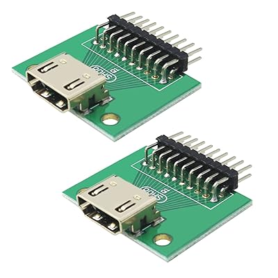
A Test Socket PCB is not simply a mechanical carrier. It functions as:
-
The electrical transition layer between socket contacts and test systems
-
A power and ground distribution platform
-
A mechanical reference surface that defines socket alignment
Its performance determines whether the socket can operate reliably throughout its service life.
Contact Consistency: The Core Challenge
Over time, socket contacts experience wear, oxidation, and mechanical fatigue. A poorly designed Test Socket PCB can amplify these issues by:
-
Uneven contact force distribution
-
Localized board flexing
-
Misalignment between socket and DUT
A robust PCB design ensures uniform mechanical support, helping maintain stable contact resistance.
Signal Degradation Across Socket Interfaces
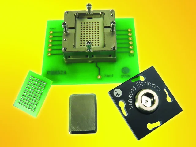
At high data rates, the socket-to-PCB transition becomes a dominant source of signal degradation. Effective Test Socket PCB design focuses on:
-
Short and symmetrical signal escape routing
-
Controlled impedance immediately below the socket pins
-
Minimization of stubs and via discontinuities
These measures reduce reflection, jitter, and eye-diagram collapse during testing.
Power Delivery Under Dynamic Load Conditions
Test sockets often serve devices that switch rapidly between power states. A Test Socket PCB must handle:
-
High transient current demand
-
Fast power sequencing
-
Noise isolation between power domains
Well-designed power planes and local decoupling near the socket are essential for stable test behavior.
Mechanical Stackup and Board Stiffness
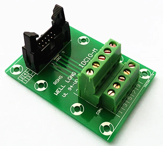
Mechanical deformation is a silent killer in socket-based testing. To prevent it, Test Socket PCBs typically use:
-
Symmetrical multilayer stackups
-
Increased board thickness or local stiffeners
-
Reinforced socket mounting regions
Controlled stiffness helps preserve flatness and coplanarity across repeated insertions.
Supporting Fine-Pitch and High-Pin-Count Sockets
As device packages evolve, test sockets follow with tighter pitch and higher pin density. Test socket PCBs must support:
-
Fine-pitch breakout routing
-
HDI structures and microvias
-
Precise hole-to-pad alignment
Manufacturing capability directly impacts socket compatibility.
Material Selection for Long-Term Stability
Material choice affects both electrical and mechanical performance. Common strategies include:
-
High-Tg FR-4 for structural durability
-
Low-loss laminates for high-speed signal paths
-
Hybrid stackups for mixed-signal test environments
Material stability extends socket service life.
Manufacturing Tolerances and Repeatability
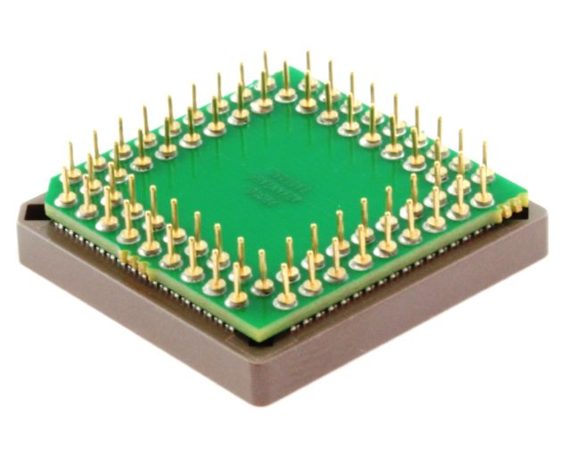
A Test Socket PCB used in production must be reproducible. Key manufacturing controls include:
-
Tight thickness and flatness tolerances
-
Consistent plating quality
-
Electrical continuity and impedance verification
Repeatability ensures that replacement boards behave identically in the test system.
Where Test Socket PCBs Are Commonly Used
Test Socket PCBs are widely deployed in:
-
High-volume final test lines
-
System-level test (SLT) platforms
-
Memory and processor production testing
-
Automotive-grade semiconductor validation
In these environments, uptime and consistency are critical.
Selecting a Test Socket PCB Manufacturing Partner
An experienced Test Socket PCB manufacturer should offer:
-
Proven socket integration experience
-
High pin count and impedance control capability
-
Mechanical and material engineering support
-
Stable quality across repeated production lots
The right partner helps reduce maintenance cost and yield loss.
Conclusion
The Test Socket PCB is a key enabler of reliable, repeatable semiconductor testing. By controlling contact consistency, signal degradation, mechanical stability, and manufacturing repeatability, a well-designed test socket PCB ensures long-term performance in high-cycle production environments.
Working with an experienced Test Socket PCB supplier is essential for sustaining test quality and production efficiency.
