Customer CaseElectronics Industry NewsEngineering TechnologiesPCB DesignPCB ManufacturingPCB Materials
High Speed Test PCB: Precision PCB Solutions for High-Speed Signal Validation
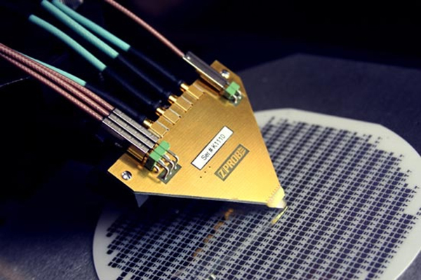
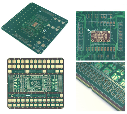
As data rates continue to increase across semiconductor and high-speed electronics, accurate testing becomes more challenging. High Speed Test PCBs are engineered to support multi-gigabit signal transmission, low jitter, and precise impedance control, ensuring reliable validation in demanding test environments. These specialized PCBs are widely used in semiconductor testing, ATE systems, and high-speed interface verification....