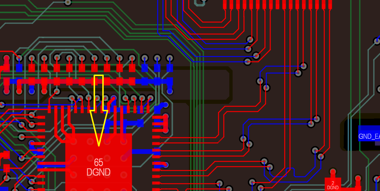
RF Routing - KKPCB
 
HomeTag

RF Routing - KKPCB

Engineering Double Layer HF PCB for Ultra-Stable RF Performance and Low-Loss Microwave Signal Integrity

As RF communication, IoT edge devices, automotive radar, and compact wireless modules continue to evolve, the Double Layer HF PCB has become a preferred architecture for delivering high-frequency stability, low insertion loss, and predictable electromagnetic performance. Although limited to two copper layers, a Double Layer HF PCB—when engineered correctly—can outperform many multilayer structures in signal...

RF PCB Design for 5G Devices: Antenna Integration, Impedance Control & High-Frequency Layout Guide

RF PCB Design for 5G Devices: High-Frequency Architecture, Antenna Integration & Engineering Best Practices Designing RF PCBs for 5G hardware is far more than simple high-speed layout—it requires a deep command of electromagnetic behavior, antenna engineering, high-frequency signal routing, impedance control, and noise isolation.In next-generation wireless systems, the antenna is no longer a passive component—it...