phase stability - KKPCB
 
HomeTag

phase stability - KKPCB

Maximize RF Power Handling and Phase Stability Using RO4350B PCB Laminates in High-Frequency Antenna Modulegs

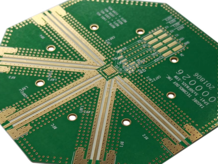
Modern wireless systems—from 5G radio units and phased-array antenna modules to automotive radar and satellite communication terminals—demand PCBs that deliver high RF power handling, exceptional phase stability, and ultra-low loss. As antenna modules continue to shrink while operating at higher frequencies, selecting the correct laminate becomes a mission-critical design decision. Among all mid-frequency RF substrates,...

Minimize Crosstalk and Maintain Impedance Precision Using Advanced Blind Via PCB Layouts in 5G mmWave Systems

5G mmWave hardware doesn’t leave much room for layout mistakes. When operating above 24 GHz, a few microns of misalignment, a poorly shaped via stub, or an uncontrolled dielectric transition can collapse RF integrity. That is why advanced blind via PCB layouts have become a core enabling technology for minimizing crosstalk, stabilizing impedance, and preserving...

Optimize RF Transmission and Phase Consistency Using High-Frequency Sensor PCB Laminates in Automotive ADAS Sensing Modules

Next-generation automotive ADAS sensing modules, including 77–81 GHz radar, LiDAR, and mmWave sensor arrays, require PCBs with ultra-stable dielectric properties, low insertion loss, and phase-coherent RF routing. Performance depends on maintaining consistent Dk/Df, low-loss mmWave signal propagation, and minimal EMI, even under harsh thermal cycling, vibration, and humidity conditions in vehicles.   High-frequency sensor PCB...

Reduce Electromagnetic Drift and Improve Wideband Sensitivity Through High Frequency Sensor PCB Engineering for Medical Diagnostic Sensors

Medical diagnostic sensors have shifted toward high-frequency, microwave-based detection architectures to improve resolution, penetration depth, and signal precision. High Frequency Sensor PCB platforms now form the RF backbone of sensing modules used in MRI coils, millimeter-wave tissue scanners, microwave breast-imaging units, vital-sign monitoring radars, and non-contact biomedical sensors. These RF sensor PCB systems require extremely...

Stabilize Wideband Impedance and Reduce Signal Drift Using RO4835 PCB Laminates in Mission-Critical Satellite Links

Satellite communication hardware depends on highly stable RF PCB materials capable of maintaining low-loss transmission, tight impedance control, and long-term dielectric stability under extreme environmental shifts. RO4835 PCB laminates—known for oxidation-resistant resin systems, stable Dk over temperature, and low insertion loss up to Ka-band—are frequently selected for mission-critical RF payloads, transceiver modules, phased arrays, and...

Optimizing High-Frequency Stability and Low-Loss Transmission Using RF-35 PCB Laminates for Modern Wireless Systems

RF-35 PCB laminates operate in a class where dielectric precision directly shapes RF linearity, bandwidth uniformity, and system-level efficiency. Modern wireless products—Wi-Fi 6/7 modules, IoT gateways, sub-6 GHz links, and microwave-band transceivers—depend on stable Dk/Df behavior to maintain predictable impedance and low insertion loss. RF-35 offers a low-loss dielectric platform designed for controlled RF propagation,...

Enhance Signal Integrity and Power Density with RO4350B PCB Designs in 5G Smartphone RF Front-Ends

RO4350B PCB materials are widely deployed in 5G smartphone RF front-end modules because they provide a balanced dielectric profile, low-loss characteristics, and stable RF transmission up to sub-6 GHz and selected mmWave bands. Modern antenna arrays, PA/LPF modules, LNA chains, and tunable impedance networks face stringent constraints in signal integrity, power density, EMI coupling, and...

High-Frequency Signal Integrity Optimization and Phase-Stable Transmission with Megtron 7 PCB Substrates in 5G Server and High-Speed Computing Systems

Megtron 7 PCB laminates are widely adopted in 5G servers, AI computing accelerators, and cloud networking equipment due to their exceptionally low dielectric loss and superior stability at 28–112 Gbps PAM4 and mmWave bands. As system architectures transition toward high-density multi-lane SerDes and advanced RF interconnects, PCB materials become a primary constraint influencing channel loss...

Hybrid Stackup and Miniaturized RF Design with PTFE PCBs in Next-Generation 5G Base Stations

1. Engineering Overview   Next-generation 5G base stations require high-density, miniaturized RF front-end modules with low insertion loss, precise impedance, and stable phase performance across mmWave bands (28–39 GHz).   PTFE PCB laminates, with Dk = 2.15 ± 0.02 and Df = 0.0009 @10GHz, provide superior dielectric consistency and thermal stability for tightly packed MIMO...

Dielectric Uniformity and Manufacturing Precision of PTFE PCBs for Aerospace Communication Equipment

1. Engineering Overview   Modern aerospace RF communication equipment, including satellite transceivers and spaceborne antenna modules, demands ultra-low-loss PTFE PCBs with tight dielectric uniformity and precise manufacturing tolerances. Small variations in Dk or CTE can lead to phase drift, impedance mismatch, and degraded link margin in Ku/Ka-band RF payloads.   PTFE PCB laminates, with Dk...