multilayer PCB stackup - KKPCB
 
HomeTag

multilayer PCB stackup - KKPCB

Power Integrity PCB: Ensuring Stable Power Delivery for High-Speed Electronics

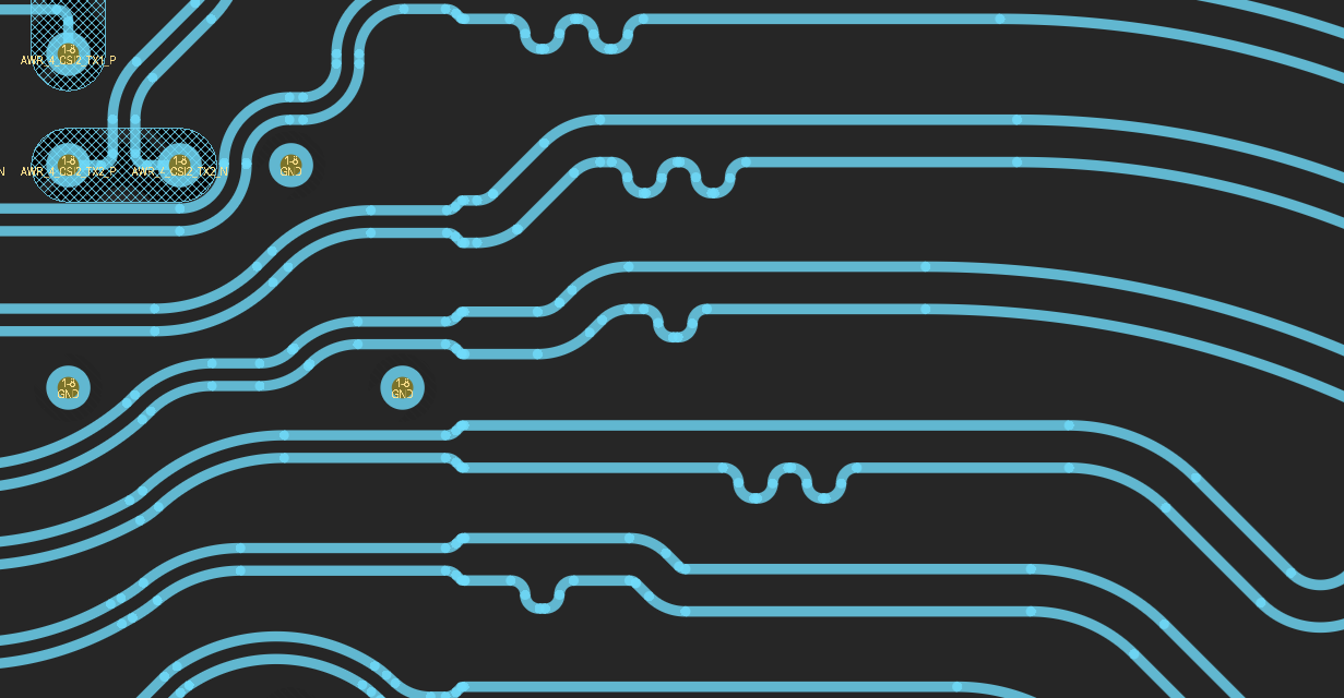
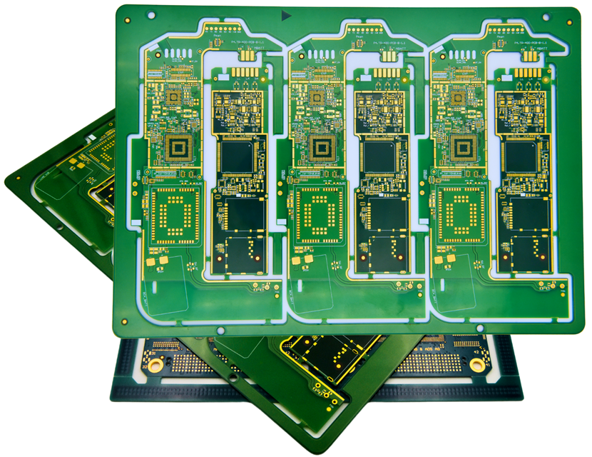
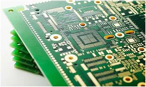
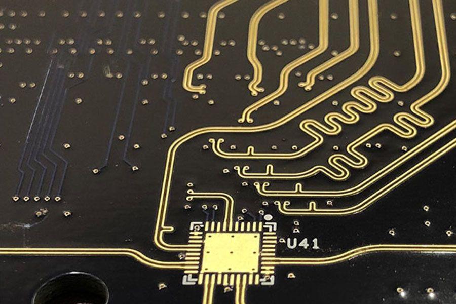
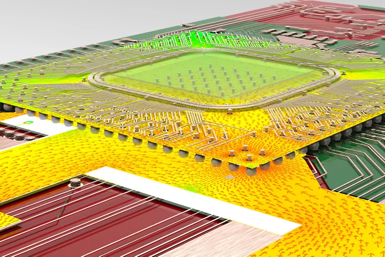
Power Integrity PCB: Ensuring Stable Power Delivery for High-Speed Electronics As modern electronic systems operate at increasingly high speeds, maintaining Power Integrity (PI) on printed circuit boards is critical. Power Integrity PCB design ensures that all components receive clean, stable voltage, minimizing noise, voltage drop, and electromagnetic interference (EMI). Poor power integrity can cause timing...

Differential Pair PCB: Design Guidelines for High-Speed Signal Integrity

Differential Pair PCB: Design Guidelines for High-Speed Signal Integrity In modern high-speed digital systems, Differential Pair PCB routing has become a fundamental design technique for maintaining signal integrity and reducing electromagnetic interference. Interfaces such as USB, HDMI, PCIe, Ethernet, and high-speed SerDes rely heavily on differential signaling to achieve reliable high-speed data transmission. A well-designed...

Why Multilayer PCBs Are Essential for High-Speed and High-Density Electronics

As electronic devices continue to evolve toward higher performance and smaller form factors, traditional two-layer circuit boards are no longer sufficient for many modern applications. This is where multilayer PCBs play a crucial role. By integrating multiple conductive layers into a single compact structure, multilayer PCBs enable engineers to design complex circuits while maintaining signal...

Optimize Phase-Stable High-Frequency Routing with Blind Via PCB Architectures in Compact Satellite Communication Payloads

Compact satellite communication payloads require precise, phase-stable RF routing to maintain signal fidelity and low insertion loss across high-frequency channels. The limited space and high-density requirements make blind via architectures essential for multilayer PCBs, enabling signal interconnects without penetrating all layers, reducing parasitic capacitance, and controlling crosstalk. Blind via PCBs allow compact routing of RF...

Improve Multi-Gigabit Transmission and Low-Loss Routing Through Impedance Controlled PCB Engineering for Data Center Switches

Modern data center switches demand high-speed, multi-gigabit transmission across densely packed PCB layers. Maintaining low insertion loss, tight impedance control, and minimal crosstalk is critical to guarantee reliable signal integrity, reduce latency, and preserve network throughput. Impedance-controlled PCB architectures provide predictable high-frequency performance for differential pair routing and dense multilayer stackups. KKPCB leverages precision lamination,...