Multilayer HDI PCB - KKPCB
 
HomeTag

Multilayer HDI PCB - KKPCB

HDI PCB: Design, Microvia Technology, and High-Density Applications

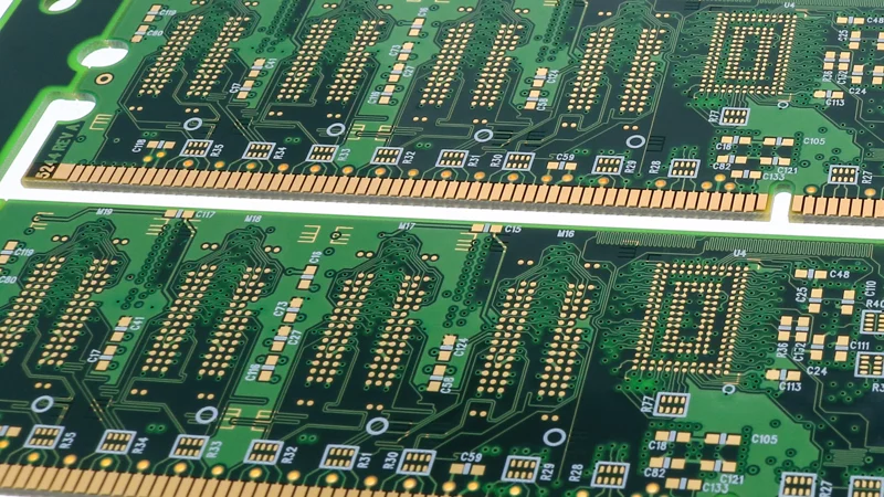
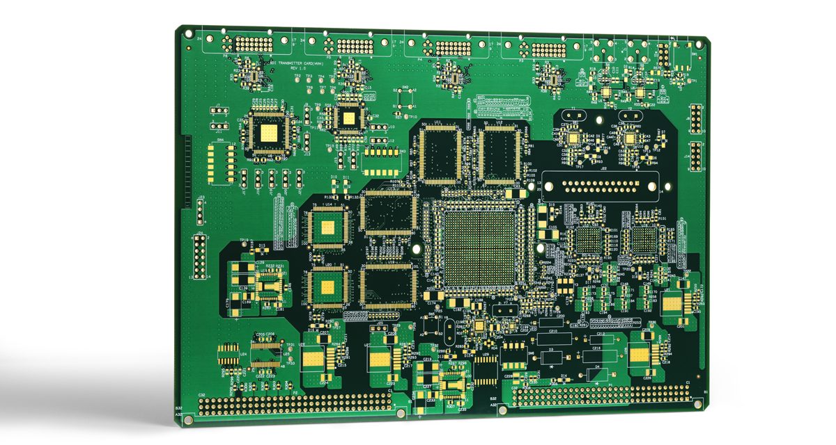
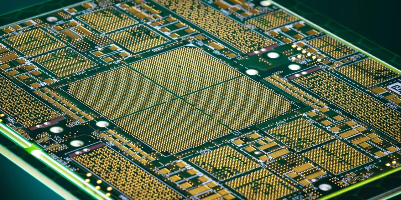
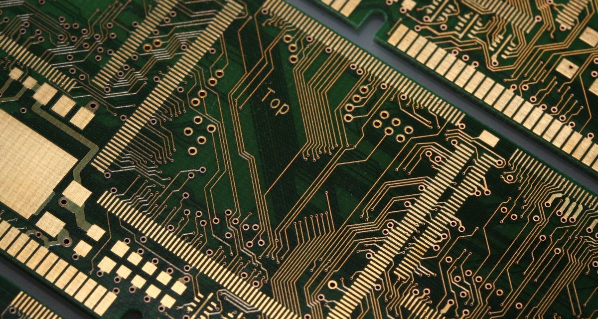
High Density Interconnect (HDI) PCB technology is designed to support modern electronic devices that demand higher performance, smaller form factors, and greater circuit complexity. HDI PCBs use advanced manufacturing techniques such as microvias, blind vias, buried vias, and fine line routing to increase the wiring density compared to traditional multilayer PCBs. As electronic products continue...

HDI PCB: High Density Interconnect PCB Manufacturing for Advanced Electronic Applications

An HDI PCB (High Density Interconnect PCB) is a key technology enabling compact, lightweight, and high-performance electronic products. As electronic devices continue to evolve toward smaller form factors, higher functionality, and faster data transmission, traditional PCB designs can no longer meet density and routing requirements. HDI PCB technology provides higher wiring density per unit area...

HDI PCB: High-Density Interconnect Technology for Compact and High-Performance Electronics

As electronic products continue to become smaller, faster, and more complex, traditional PCB technology often reaches its physical limits. HDI PCB (High-Density Interconnect PCB) technology was developed to overcome these constraints by enabling much higher routing density, improved signal integrity, and greater design flexibility. Today, HDI PCBs are widely used in high-speed digital systems, semiconductor...

HDI circuit board: the technology bridge to the future

With the continuous development of science and technology, the functional requirements of electronic devices are also constantly increasing. In order to meet this demand, HDI (High Density Interconnect) circuit boards came into being.  have attracted much attention for their high density, high performance and high reliability, and have become an important bridge connecting future technologies....