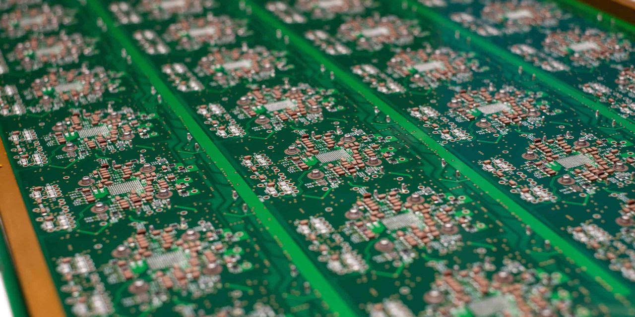
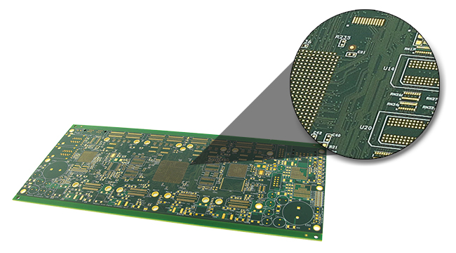
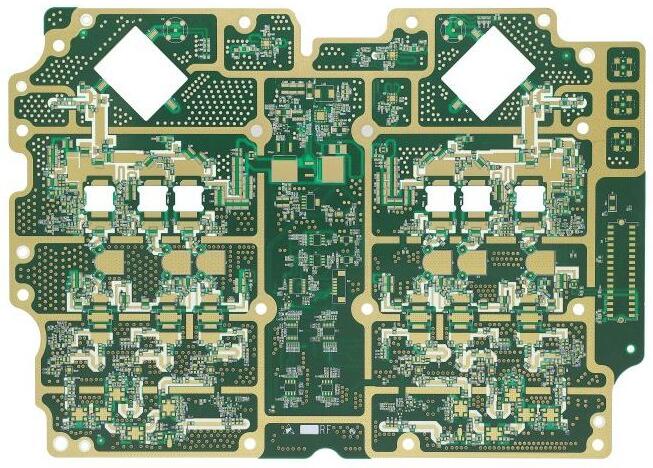
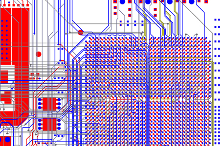
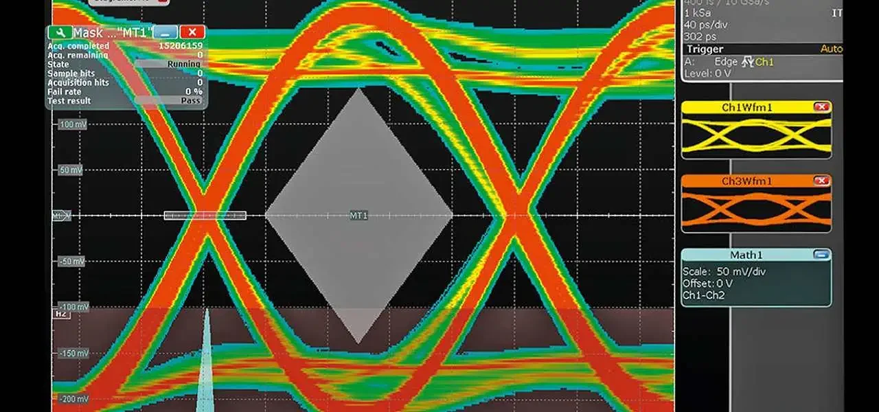
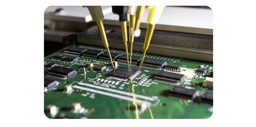
KKPCB - KKPCB
 
HomeTag

KKPCB - KKPCB

High Frequency Laminates for Signal Integrity and Low-Loss Performance in RF and Microwave PCBs

High Frequency Laminates are specialized PCB substrates engineered to deliver low dielectric loss, stable dielectric constant (Dk), and superior signal integrity in RF, microwave, and high-speed digital applications. Unlike conventional FR-4 materials, high frequency laminates maintain predictable electrical behavior across GHz and mmWave frequencies, enabling advanced communication, radar, and aerospace systems. Material Characteristics High frequency...

BT Epoxy PCB Design for Dimensional Stability and Electrical Reliability in IC Packaging Applications

A BT Epoxy PCB is a specialized organic substrate widely used in IC packaging, semiconductor interposers, and high-density electronic modules. BT (Bismaleimide Triazine) epoxy resin materials are engineered to provide enhanced thermal stability, low moisture absorption, and excellent dimensional control, making BT Epoxy PCBs a preferred choice for fine-pitch and high-I/O-count packaging environments. Unlike standard...

Material-Driven Aluminum Nitride PCB Design for Thermal and Electrical Stability

An Aluminum Nitride PCB (AlN PCB) is a ceramic-based circuit substrate engineered for electronic systems that demand exceptional thermal conductivity, electrical insulation, and dimensional stability under high power density and elevated temperature conditions. In power electronics and high-reliability applications, material selection is not a secondary decision—it defines system performance limits. Material-driven Aluminum Nitride PCB design...

Designing Ceramic PCBs for Efficient Heat Dissipation in Power and High-Voltage Electronics

A Ceramic PCB is a high-performance circuit substrate engineered for applications that demand excellent thermal conductivity, electrical insulation, and long-term reliability under harsh operating conditions. Unlike organic PCB materials such as FR-4 or PTFE, ceramic PCB substrates are inorganic, enabling stable electrical and mechanical performance at elevated temperatures and high power densities. Ceramic PCB technology...

PTFE PCB Engineering for Ultra-Low Loss and High-Frequency Signal Integrity in RF and Microwave Applications

A PTFE PCB is a critical technology platform for RF, microwave, and high-frequency electronic systems where low signal loss, phase stability, and dielectric consistency are non-negotiable. Compared with conventional FR-4 materials, PTFE PCB laminates offer significantly lower dielectric constant (Dk) and dissipation factor (Df), enabling superior signal integrity at GHz and mmWave frequencies. In modern...

Designing Automated Test Equipment PCBs for Signal Integrity, Timing Accuracy, and Long-Term Test Reliability

Automated Test Equipment (ATE) systems place some of the most demanding electrical and mechanical requirements on PCB design. An Electrical Requirements in  must simultaneously support high-speed digital interfaces, precision analog measurement paths, high pin-count connectivity, and long-term operational stability under continuous duty cycles. Unlike consumer or general industrial electronics, ATE PCBs function as measurement instruments,...

Buy High Frequency PCBs Optimized for Controlled Impedance and Low Insertion Loss in 5G and Satellite Systems

As 5G wireless infrastructure and satellite communication systems continue to evolve toward higher frequencies, wider bandwidths, and denser integration, the demand to buy high frequency PCBs with precise electrical control has increased significantly. In these applications, controlled impedance PCB design and ultra-low insertion loss PCB performance are no longer optional—they are fundamental to achieving stable...

Designing Buried Via PCBs for High-Density Routing and Signal Integrity Optimization

As electronic systems continue to evolve toward higher speed, smaller form factors, and increased functionality, traditional through-hole via structures are becoming a limiting factor. Buried Via PCB technology has emerged as a critical enabler for high-density routing and signal integrity optimization, particularly in HDI, high-speed digital, and RF applications. By embedding vias between inner layers...

Small Batch PCB Manufacturing: Enabling Flexible Engineering Validation and Low-Risk Product Development

Why Small Batch PCB Matters in Modern Electronics Development In today’s electronics industry, product lifecycles are shorter and design iterations are more frequent. Before committing to mass production, engineering teams must validate signal integrity, power stability, thermal behavior, and manufacturability. Small batch PCB manufacturing plays a critical role in this phase by enabling controlled, low-risk...

PCB Turnkey Solutions: Streamlining Electronics Manufacturing from Design to Finished Assembly

Why PCB Turnkey Matters in Modern Electronics Manufacturing As electronic systems become more complex, managing separate suppliers for PCB fabrication, component sourcing, assembly, and testing introduces cost risk, schedule delays, and quality uncertainty. This is especially true for products involving high-speed digital signals, RF circuits, power electronics, or mixed-technology assemblies. PCB turnkey solutions address this...