
Engineering Context
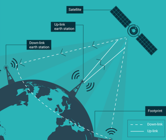
Satellite communication and aerospace systems represent some of the most demanding environments for PCB technology. Unlike terrestrial electronics, satellite PCBs must operate reliably under vacuum conditions, extreme temperature fluctuations, radiation exposure, mechanical vibration, and long-duration missions where maintenance and repair are impossible.
A Satellite PCB is not simply a conventional high-frequency circuit board. It is a mission-critical electronic platform responsible for signal transmission, power management, telemetry processing, navigation control, and communication payload operation. The PCB design must achieve excellent signal integrity, low insertion loss, thermal stability, and mechanical reliability throughout the entire mission lifecycle.
Modern satellite systems increasingly rely on high-frequency communication bands including X-band, Ku-band, and Ka-band. These applications require advanced RF PCB technologies capable of maintaining phase consistency and impedance control at GHz frequencies. Small variations in dielectric properties, copper roughness, or layer alignment can lead to signal degradation, reduced link margin, and communication errors.
For aerospace engineers and procurement teams, selecting the correct PCB manufacturer is critical. The supplier must have capabilities in high-frequency material processing, precision multilayer fabrication, reliability testing, and aerospace-level quality control.
KKCPB provides high-reliability Satellite PCB manufacturing solutions using advanced RF materials, controlled impedance processes, precision lamination technology, and simulation-driven engineering validation to support next-generation space communication systems.
Core Engineering Challenges
| Engineering Challenge | Root Cause | Engineering Impact |
|---|---|---|
| Signal degradation at high frequency | Dielectric loss and copper roughness | Reduced communication range and link margin |
| Phase instability | Material variation and thermal expansion | Beamforming accuracy reduction |
| Impedance variation | Stackup tolerance and manufacturing deviation | Increased reflection and signal distortion |
| Thermal stress | Extreme temperature cycling in space | Layer deformation and reliability risks |
| Radiation and vacuum exposure | Space environment conditions | Material degradation and performance drift |
| Mechanical vibration | Launch acceleration and shock | Via fatigue and solder joint failure |
These challenges make Satellite PCB manufacturing one of the most technically demanding segments of the PCB industry.
Aerospace communication systems require consistent electrical performance from prototype development through volume production, requiring strict process control and complete engineering verification.
Material Science & Dielectric Performance of Satellite PCB Substrates
Satellite communication PCBs commonly use advanced low-loss materials such as ceramic substrates, PTFE laminates, Rogers RF materials, and high-performance aerospace-grade laminates.
Material selection directly affects RF performance, thermal reliability, and mission lifetime.
High-Reliability Satellite PCB Material Parameters
| Parameter | Typical Requirement | Engineering Benefit |
|---|---|---|
| Dielectric Constant (Dk) Stability | ±0.05 or better | Maintains impedance accuracy |
| Dissipation Factor (Df) | <0.002 @10 GHz | Reduces insertion loss |
| Thermal Conductivity | High | Improves heat dissipation |
| CTE Stability | Low ppm/°C | Prevents layer mismatch |
| Moisture Absorption | <0.05% | Maintains dielectric consistency |
| Outgassing Performance | Low TML/CVCM | Suitable for vacuum environment |
Compared with conventional FR-4 materials, aerospace-grade RF laminates provide superior low-loss transmission and phase stability.
For high-frequency payload applications, materials such as RO3003 PCB, RO5880 PCB, ceramic PCB, and PTFE PCB are commonly selected due to their stable dielectric performance.
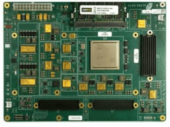
KKCPB Case Study — Satellite Communication Ku-Band Payload PCB
Client & Application Context
A satellite system integrator required a high-reliability PCB platform for a Ku-band communication payload used in a commercial Earth observation satellite.
The PCB design requirements included:
- Ku-band RF transceiver operation
- Multi-channel antenna feed network
- High-frequency signal routing
- Long-duration operation in vacuum conditions
- Extremely stable phase performance
- Radiation-resistant material selection
The customer required a PCB supplier capable of supporting both engineering development and production-level reliability validation.
Engineering Problem
The previous PCB design experienced several performance limitations:
- RF insertion loss above specification at 14 GHz
- Impedance variation exceeding ±5%
- Phase deviation between RF channels
- Thermal expansion mismatch during temperature cycling
- EMI coupling between adjacent communication channels
These issues reduced communication efficiency and created additional calibration requirements during satellite integration.
KKCPB Engineering Solution
KKCPB developed a satellite-grade RF PCB solution:
- Selected low-loss ceramic-based RF material for critical signal layers
- Designed controlled impedance transmission lines
- Optimized multilayer hybrid stackup structure
- Reduced copper surface roughness for lower conductor loss
- Applied precision vacuum lamination technology
- Implemented ground plane segmentation for EMI suppression
- Added RF test coupons for TDR and VNA verification
The RF structure was optimized through electromagnetic simulation before fabrication.
Measured Results
| Parameter | Target | KKCPB Result |
|---|---|---|
| Impedance Variation | ±5% | ±1.7% |
| Insertion Loss @14 GHz | <0.35 dB/in | 0.24 dB/in |
| Phase Deviation | <1° | 0.48° |
| Return Loss (S11) | < -15 dB | -18.2 dB |
| Layer Registration | ±30 μm | ±15 μm |
| Thermal Warpage | <0.15 mm | 0.08 mm |
Outcome
The Satellite PCB solution successfully achieved stable RF transmission performance and improved communication payload reliability.
The optimized stackup reduced signal loss and phase variation, improving antenna array consistency and reducing system-level calibration requirements.
For the satellite manufacturer, the improved PCB reliability contributed to:
- Longer mission lifetime
- Reduced integration risk
- Higher communication efficiency
- Lower maintenance requirements after launch
Stackup Design & RF Implementation
Representative 8-Layer Satellite RF PCB Stackup
| Layer | Function | Material |
|---|---|---|
| L1 | RF Signal Layer | Ceramic RF Laminate |
| L2 | Ground Plane | High conductivity Copper |
| L3 | RF Routing Layer | Low-Loss PTFE Material |
| L4 | Power Distribution | High Reliability Laminate |
| L5 | Digital Control Signals | Aerospace Grade Material |
| L6 | Ground Shield Layer | Copper |
| L7 | RF Interface Layer | Ceramic PCB |
| L8 | Mechanical Support | High-Tg Aerospace Material |
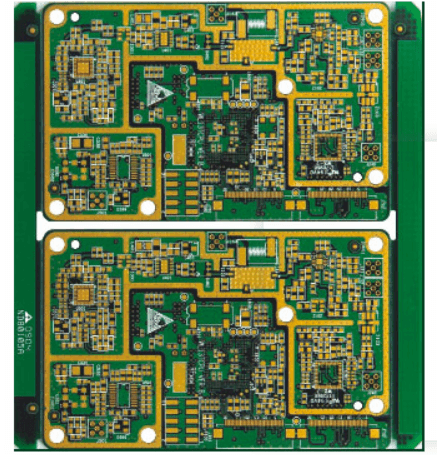
To ensure satellite-level RF performance, KKCPB performs comprehensive engineering verification.
HFSS Electromagnetic Simulation
Used for:
- RF field distribution analysis
- Antenna feed optimization
- EMI coupling evaluation
- High-frequency transmission simulation
ADS Circuit Simulation
Used for:
- S-parameter optimization
- Phase matching analysis
- RF network performance prediction
TDR Measurement
Used for:
- Controlled impedance verification
- Transmission line discontinuity detection
Thermal FEM Simulation
Used for:
- Thermal expansion analysis
- Heat distribution prediction
- Material reliability evaluation under extreme conditions
Simulation results are correlated with physical measurements to ensure production consistency.
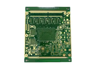
Environmental & Reliability Validation
Space electronics require extensive reliability verification before deployment.
| Test | Condition | Result |
|---|---|---|
| Thermal Cycling | -55°C ↔ +125°C, 1000 cycles | No delamination |
| Vacuum Outgassing | Aerospace requirement | Passed |
| Humidity Test | 85°C / 85% RH | Stable dielectric properties |
| Vibration Test | Launch vibration profile | No mechanical failure |
| Shock Test | High acceleration impact | No crack formation |
| Solder Reflow | 260°C ×3 cycles | No layer separation |
| Radiation Exposure | Mission-level testing | Electrical stability maintained |
These reliability tests confirm that KKCPB Satellite PCB solutions can withstand demanding aerospace environments.
Engineering Summary & Contact
Satellite PCB technology requires a combination of advanced material science, precision manufacturing, and rigorous reliability validation. High-frequency aerospace systems depend on stable dielectric properties, controlled impedance, low-loss transmission, and excellent thermal performance.
From communication satellites and RF payload units to aerospace electronic systems, PCB reliability directly influences mission success.
KKCPB specializes in high-reliability Satellite PCB manufacturing, providing RF stackup optimization, low-loss material processing, precision multilayer fabrication, and complete engineering verification.
With expertise in RF PCB, Microwave PCB, Ceramic PCB, PTFE PCB, and high-frequency communication systems, KKCPB supports aerospace customers in developing reliable PCB solutions for next-generation space applications.
