IoT PCB - KKPCB
 
HomeTag

IoT PCB - KKPCB

Fine Line PCB: Precision Routing for High-Density and High-Speed Electronics

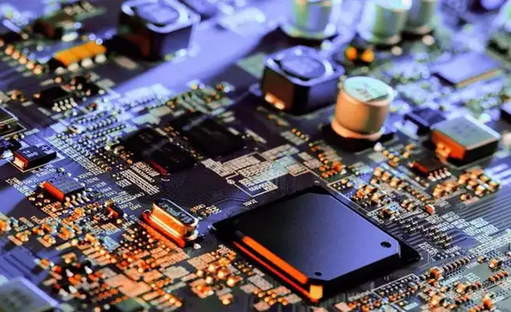
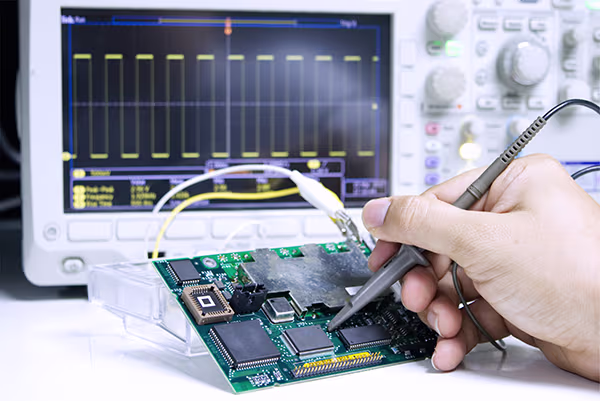
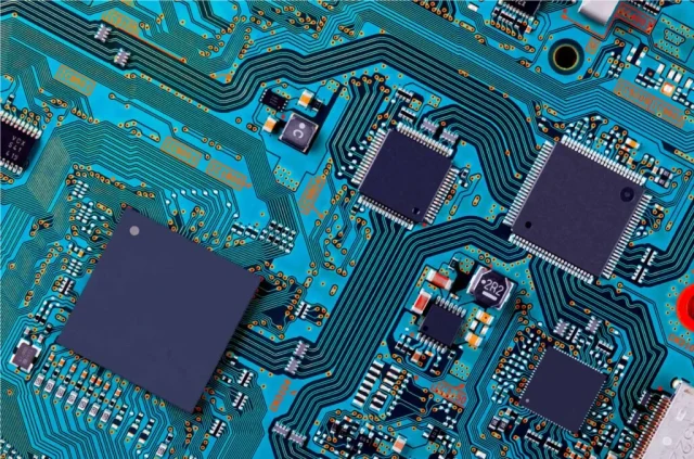
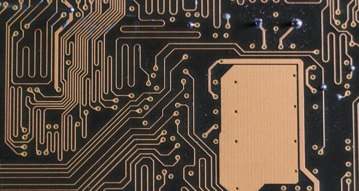
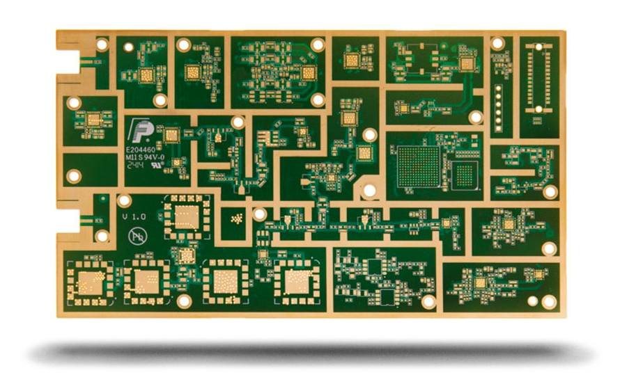
What Is a Fine Line PCB? A Fine Line PCB is a printed circuit board designed with ultra-thin traces and narrow spacing, typically under 4 mils (0.1 mm), enabling high-density interconnections for compact electronic devices. Fine line PCBs are essential in applications where space constraints, high-speed signals, and precise routing are required, such as 5G...

High Speed Logic PCB: Ensuring Signal Integrity and Reliable Digital Performance

What Is a High Speed Logic PCB? A High Speed Logic PCB is a printed circuit board engineered to handle high-frequency digital signals with minimal distortion, noise, or timing errors. These PCBs are critical in applications where fast signal transitions, high data rates, and precise timing are required, such as computer motherboards, networking equipment, 5G...

Power Integrity PCB: Ensuring Stable Voltage and Reliable High-Speed Electronics

What Is a Power Integrity PCB? A Power Integrity PCB (PI PCB) is designed to maintain stable voltage, low noise, and reliable power delivery across high-speed circuits and high-density electronic systems. In modern electronics, where switching speeds are faster and current densities higher, power integrity is crucial to avoid voltage drops, ground bounce, and signal...

Fine Line PCB: High-Density, High-Precision PCB Solutions for Advanced Electronics

What Is a Fine Line PCB? A Fine Line PCB is a printed circuit board designed with ultra-narrow traces and spacing, typically below 100 µm. This allows for high-density component placement, complex routing, and miniaturized PCB designs. Fine line PCBs are essential in high-speed digital, RF, 5G, IoT, and aerospace electronics, where both signal integrity...

High Speed Logic PCB: Optimized Design for Fast Digital Circuits and Reliable Performance

Introduction to High Speed Logic PCB A High Speed Logic PCB is designed to support ultra-fast digital circuits while maintaining signal integrity, low noise, and reliable operation. These PCBs are critical for modern electronics, where data rates and clock frequencies are continually increasing, such as in computing, networking, 5G communications, automotive ECUs, and IoT devices....

Power Integrity PCB: Ensuring Stable Voltage and Reliable Performance in High-Speed Electronics

What Is a Power Integrity PCB? A Power Integrity (PI) PCB is engineered to ensure stable and reliable voltage delivery across the entire printed circuit board. In modern electronics, high-speed digital, RF, 5G, IoT, and high-performance computing systems demand consistent voltage and low noise on power planes. A Power Integrity PCB minimizes voltage ripple, power...

Signal Integrity PCB: Ensuring High-Speed, Low-Noise Performance in Advanced Electronics

What Is a Signal Integrity PCB? A Signal Integrity PCB is engineered to maintain clean, reliable, and distortion-free signal transmission in high-speed and high-frequency electronic systems. Signal degradation, crosstalk, and reflections can compromise system performance, especially in high-speed digital, RF, 5G, IoT, and high-performance computing applications. Signal integrity PCB design ensures consistent impedance, controlled trace...

Differential Pair PCB: High-Speed PCB Design for Signal Integrity and Noise Reduction

What Is a Differential Pair PCB? A Differential Pair PCB is a specialized printed circuit board designed with paired traces carrying equal and opposite signals. This design minimizes electromagnetic interference (EMI), reduces signal crosstalk, and maintains high-speed signal integrity. Differential pair PCBs are critical in applications where accurate high-speed data transmission is required, such as...

Fine Line PCB: High-Density, Precision PCB Solutions for Advanced Electronics

What Is a Fine Line PCB? A Fine Line PCB is a printed circuit board engineered with ultra-narrow traces and tight spacing, typically below 100 µm. This enables high-density routing and compact component placement while maintaining excellent signal integrity and reliability. Fine line PCBs are essential in high-speed digital systems, RF modules, 5G devices, IoT...

Low Loss PCB: Advanced PCB Technology for High-Speed, RF, and High-Frequency Applications

A Low Loss PCB is a specialized printed circuit board designed to reduce dielectric loss, insertion loss, and signal distortion in high-speed and high-frequency electronic systems. As modern electronics such as 5G communication systems, RF front-end modules, high-speed data transmission, and semiconductor test equipment operate at ever-increasing frequencies, signal integrity becomes a critical design challenge....