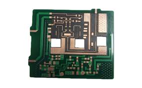
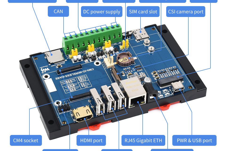
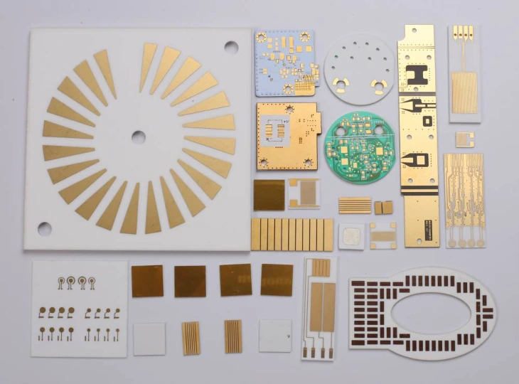
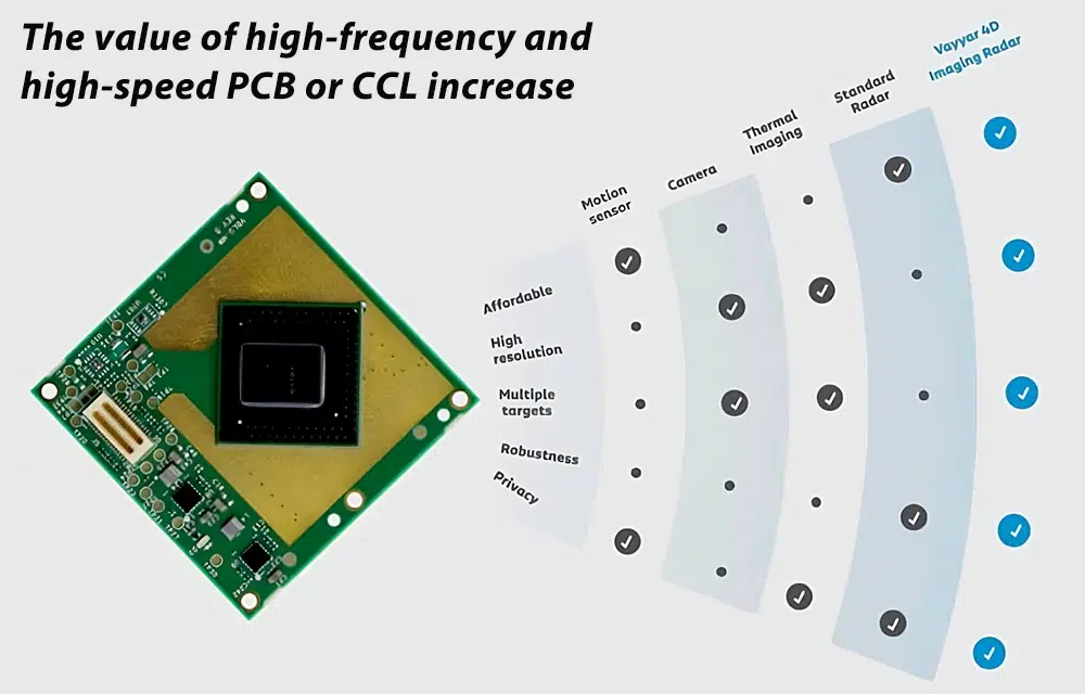
impedance control - KKPCB
 
HomeTag

impedance control - KKPCB

Dielectric Uniformity and Manufacturing Precision of PTFE PCBs for Aerospace Communication Equipment

1. Engineering Overview   Modern aerospace RF communication equipment, including satellite transceivers and spaceborne antenna modules, demands ultra-low-loss PTFE PCBs with tight dielectric uniformity and precise manufacturing tolerances. Small variations in Dk or CTE can lead to phase drift, impedance mismatch, and degraded link margin in Ku/Ka-band RF payloads.   PTFE PCB laminates, with Dk...

Low-Loss Transmission and Impedance Control of PTFE PCBs in Satellite Communication Payloads

1.Engineering Overview / Abstract   Modern satellite communication payloads operating in Ka- and Ku-band frequencies require PCB substrates with ultra-low loss, precise impedance control, and stable phase performance. PTFE PCB laminates provide an ideal platform for high-frequency RF interconnects due to their low dielectric constant (Dk = 2.10 ± 0.03) and minimal loss tangent (Df...

Impedance Control and RF Efficiency Optimization Using Ceramic PCBs in Industrial Wireless Sensor Networks

1. Engineering Overview / Abstract   As Industrial IoT communication modules become more compact and operate at higher frequencies, maintaining precise impedance control and RF efficiency is critical for reliable data transmission. Traditional polymer-based PCBs often suffer from dielectric drift, thermal warpage, and EMI coupling, which degrade signal integrity in dense wireless sensor networks.  Ceramic...

Low-Loss Transmission and Impedance Control of Megtron 7 PCBs in Automotive mmWave Radar Systems

1. Engineering Overview   Automotive mmWave radar modules for advanced driver-assistance systems (ADAS) require precise RF signal propagation with minimal loss and stable impedance across multilayer PCBs. Trace density and high-frequency operation introduce challenges in maintaining signal integrity and   crosstalk suppression. Megtron 7 PCBs, with Dk = 3.40 ±0.02 and Df = 0.0018 @ 10...

Mproving Impedance Control and Reliability of Taconic TLY-5 PCB Platforms for Medical Imaging and Diagnostic RF Modules

1. Engineering Overview / Abstract   Modern medical imaging systems — including MRI coils, ultrasound transceivers, and RF diagnostic sensors — rely on tight impedance control and ultra-low signal drift to ensure accurate imaging and patient diagnostics.  The Taconic TLY-5 PCB platform, with its Dk of 2.20 ± 0.02 and Df of 0.0009 @10GHz, provides...

Optimizing Impedance Control and Thermal Uniformity of Taconic RF-35 PCB Substrates for 5G Smartphone Antenna Modules

1. Engineering Overview / Abstract   As 5G smartphone antenna modules integrate multiple MIMO paths and beam-forming arrays, precise impedance control and thermal uniformity become critical for stable signal transmission.  Taconic RF-35 PCB substrates enable consistent dielectric performance and low-loss propagation under compact, multilayer conditions.  KKPCB engineers apply fine-tuned lamination and impedance verification processes to...

Enhancing Signal Integrity and Calibration Stability of Taconic RF-35 PCBs in Precision RF Test and Measurement Equipment

1. Engineering Overview / Abstract   As precision RF test and measurement systems extend into the 40 – 110 GHz range, achieving sub-degree phase accuracy and minimal insertion-loss drift becomes a primary design requirement.  Taconic RF-35 PCBs—engineered with a glass-reinforced PTFE composite (Dk = 3.50 ± 0.05, Df = 0.0018 @ 10 GHz)—enable calibration-grade impedance...

Enhancing Signal Integrity and RF Stability of TLY-5 PCBs in 5G Smartphone Antenna and Transceiver Modules

1. Engineering Overview — Material-Driven Signal Reliability for 5G Smartphones   As 5G smartphones evolve toward multi-antenna, wide-band, and ultra-compact RF front-end architectures, PCB materials play a decisive role in ensuring signal alignment and thermal stability.  The TLY-5 PCB, a PTFE-glass composite laminate from Taconic, provides excellent dielectric uniformity (Dk = 2.2 ± 0.02, Df...

RF Test PCB: Engineering Precision for High-Frequency Testing Systems

RF Test PCB: Engineering Precision for High-Frequency Testing Applications Introduction As wireless communication, semiconductor devices, and high-frequency electronics continue to advance, the demand for precise and reliable test platforms has increased dramatically. Among these platforms, the RF Test PCB plays a central role. It enables engineers to validate RF performance, measure high-frequency characteristics, and ensure...

Probe Card PCB: Engineering Precision for High-Accuracy Wafer-Level Semiconductor Testing

Probe Card PCB: Engineering Precision for Wafer-Level Testing Introduction At the wafer-level test stage, the probe card PCB serves as the indispensable interface between automated test equipment (ATE) and the semiconductor wafer. As device geometries continue shrinking and electrical performance requirements become more demanding, precision test interfaces have become essential. The probe card PCB establishes...