High-Precision PCB - KKPCB
 
HomeTag

High-Precision PCB - KKPCB

Probe Card PCB: Design, Materials and Manufacturing for Semiconductor Wafer Testing

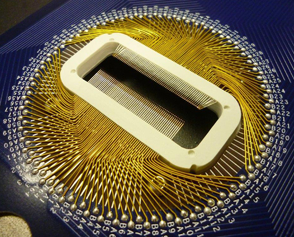
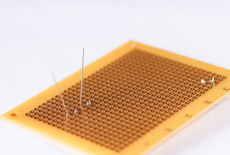
Before a semiconductor chip ever reaches packaging, it must first prove itself on the wafer. Engineers run electrical tests directly on the silicon to identify defective dies early in the manufacturing process. This delicate operation relies on a specialized testing interface known as a Probe Card. At the heart of this system lies the Probe...

Logic Test PCB: Optimizing Circuit Verification and Functional Testing

In modern digital electronics, ensuring that circuits function correctly before mass production is essential. Logic Test PCBs are specialized printed circuit boards designed to validate the functionality of digital systems, identify defects, and verify signal logic. From microcontrollers and FPGAs to high-speed memory and communication modules, Logic Test PCBs play a critical role in the...

Multilayer Test PCB – High Layer Count PCB for Precision Electronic Testing

What Is a Multilayer Test PCB? A Multilayer Test PCB is a high-layer-count printed circuit board specifically designed for electronic testing applications. It is commonly used in semiconductor ATE systems, functional testing platforms, RF validation, and high-speed device verification. Unlike standard multilayer boards used in end products, test PCBs must prioritize electrical precision, signal integrity,...

Load Board PCB – High Precision Interface Board for Semiconductor Testing

What Is a Load Board PCB? A Load Board PCB is a critical interface board used in Automated Test Equipment (ATE) systems for semiconductor device testing. It connects the tester to the device under test (DUT), transmitting signals, power, and measurement data with high accuracy and stability. Load boards are specifically engineered to support high...

ATE Test PCB – High Precision PCB for Automated Test Equipment Applications

ATE Test PCB for Semiconductor and IC Testing An ATE Test PCB (Automated Test Equipment PCB) is a high-precision printed circuit board designed for semiconductor and integrated circuit testing systems. It serves as the electrical interface between the test system and the device under test (DUT), ensuring accurate signal transmission, stable power delivery, and reliable...

Fine Line PCB: High Precision PCB Manufacturing for HDI and High-Density Routing

What Is a Fine Line PCB? A Fine Line PCB is a high-precision printed circuit board manufactured with ultra-thin trace width and tight trace spacing, enabling high-density routing for advanced electronic products. Compared with standard PCB technology, Fine Line PCB fabrication focuses on achieving smaller line/space (L/S), higher wiring density, and improved signal performance in...

Fine Line PCB: High-Density, High-Precision PCB Solutions for Advanced Electronics

What Is a Fine Line PCB? A Fine Line PCB is a printed circuit board designed with ultra-narrow traces and spacing, typically below 100 µm. This allows for high-density component placement, complex routing, and miniaturized PCB designs. Fine line PCBs are essential in high-speed digital, RF, 5G, IoT, and aerospace electronics, where both signal integrity...

Custom Probe Card PCB: High-Precision Platforms for Stable and Repeatable Wafer Testing

In wafer-level semiconductor testing, probe cards must deliver precise electrical contact across thousands of touchdowns while maintaining consistent signal performance. The Custom Probe Card PCB provides the structural and electrical foundation that supports probe arrays, ensuring accurate, repeatable wafer testing. A properly engineered custom probe card PCB directly impacts test yield, device characterization accuracy, and...

Advancing Electronic Engineering Through High-Precision PCB Prototype Fabrication Technologies

Modern electronics development depends on fast, accurate, and predictable PCB prototype fabrication. As device complexity rises—spanning RF modules, 5G transceivers, AI accelerators, and densely integrated consumer electronics—engineering teams rely on high-precision prototyping to validate architectures before mass production. PCB prototype technology has evolved from simple single-layer boards into a highly automated, material-specific, impedance-controlled manufacturing discipline....

Boost Design Accuracy and Signal Integrity Using High-Precision PCB Prototype Fabrication Technologies

High-precision PCB prototype fabrication has become the backbone of modern electronics development. As product cycles shrink and system complexity rises—spanning RF modules, high-speed digital interfaces, IoT sensors, EV power systems, and aerospace electronics—the demand for PCB prototype accuracy, signal integrity stability, and manufacturing predictability has never been higher. A high-reliability prototype is not “just a...