high density pcb - KKPCB
 
HomeTag

high density pcb - KKPCB

Buried Via PCBs: Advanced Techniques for High-Density Multilayer Boards

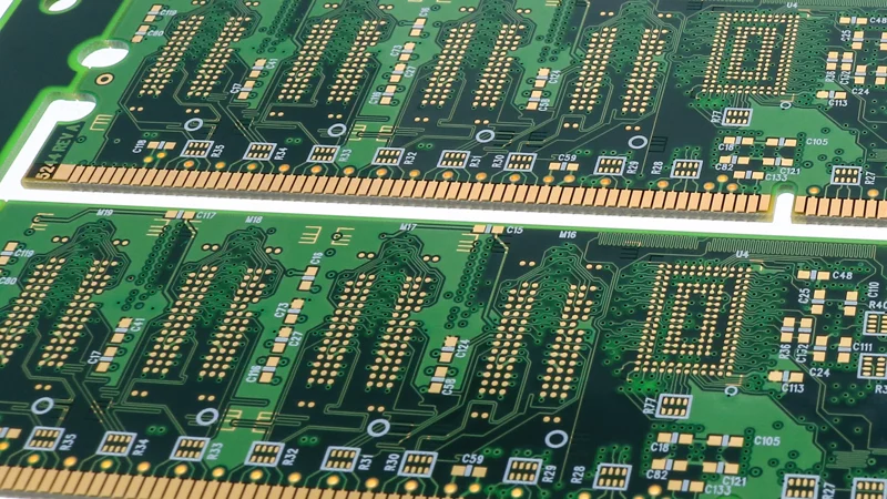
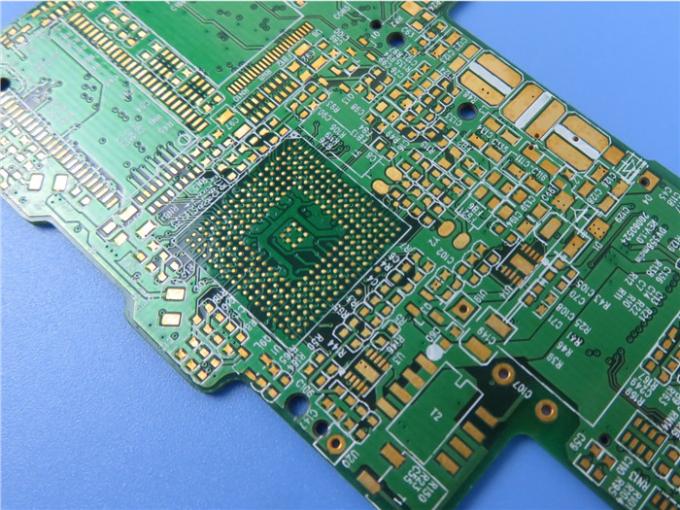
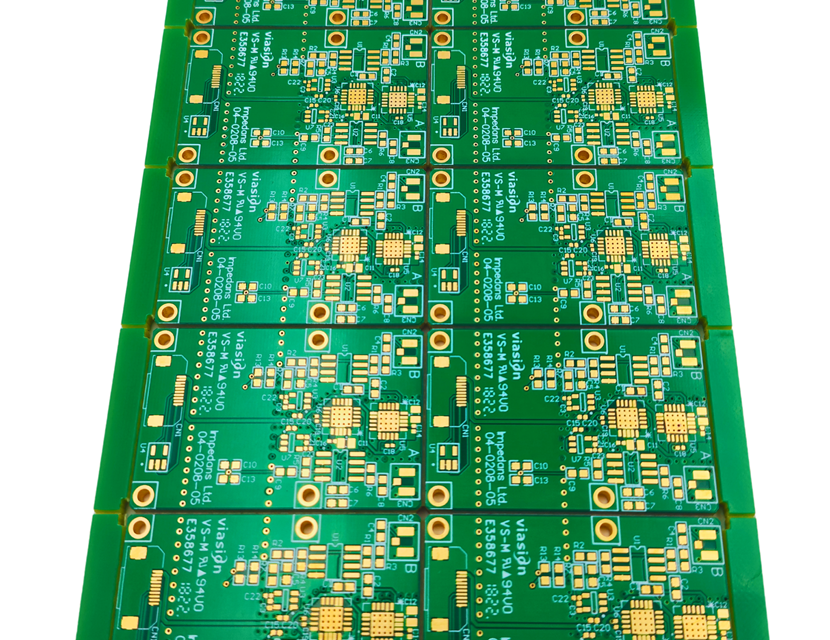
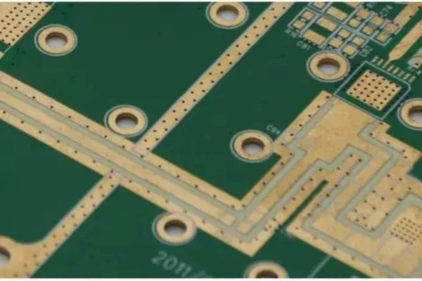
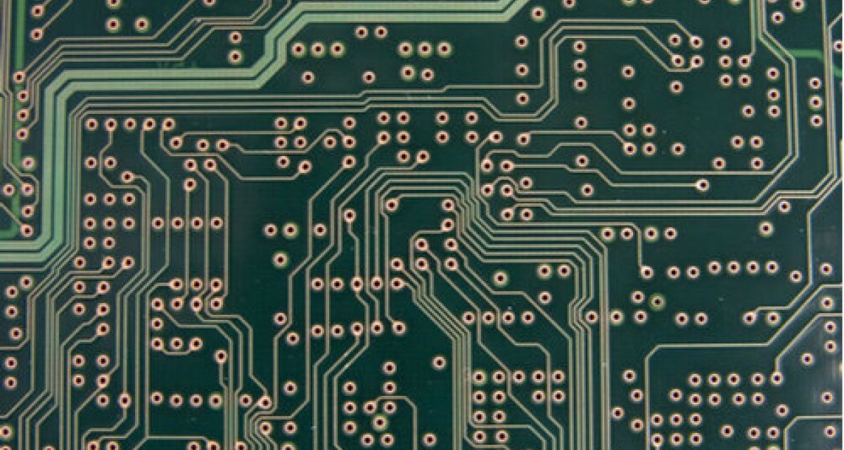
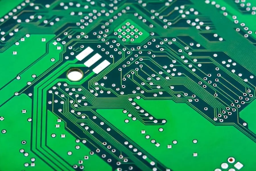
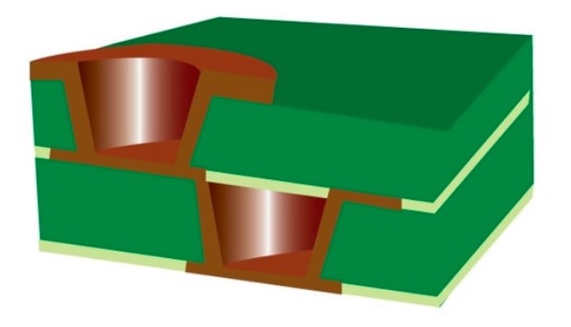
Buried via technology has become essential in modern PCB design, particularly for high-density, high-performance applications. Unlike through-hole vias that pass through all layers, buried vias connect only internal layers, leaving outer layers uninterrupted. This allows designers to maximize routing space, improve signal integrity, and achieve compact, multilayer PCB layouts. Design Advantages Maximizing Board Real Estate:By...

Buried Via PCB: Advanced Multilayer Interconnects for High-Density Electronics

As electronic devices become smaller and more complex, the need for high-density interconnections within printed circuit boards increases. Buried via PCBs offer a solution by connecting inner layers without using surface space, allowing for compact, high-performance multilayer boards. Buried vias improve routing flexibility, signal integrity, and design density, making them critical for advanced applications such...

Blind Via PCB: Advanced Interconnect Technology for High-Density Multilayer Circuit Boards

As electronic devices become smaller, faster, and more complex, PCB designers must adopt advanced interconnection technologies to achieve higher circuit density. Blind Via PCB technology is widely used in modern HDI PCB designs to enable efficient routing between layers without occupying unnecessary space on the entire board. A Blind Via PCB uses vias that connect...

High Layer Count PCB: Advanced Multilayer PCB Design for Complex Electronics

As electronic systems become more powerful and complex, standard multilayer PCBs are sometimes no longer sufficient. Advanced applications such as telecommunications infrastructure, data servers, and aerospace electronics often require extremely dense routing and precise signal control. This is where High Layer Count PCBs come into play. These circuit boards typically contain 20 layers or more,...

Multilayer PCB: Advanced Design for High-Density and High-Speed Electronics

Multilayer PCB: Advanced Design for High-Density and High-Speed Electronics With modern electronic devices becoming increasingly compact and high-performance, Multilayer PCB technology is essential for achieving complex circuit routing, improved signal integrity, and efficient power distribution. A multilayer PCB consists of three or more conductive copper layers laminated together with dielectric materials , enabling compact, high-density,...

Microvia PCB: High-Density Interconnect Solutions for Advanced Electronics

Microvia PCB: High-Density Interconnect Solutions for Advanced Electronics As electronic devices become smaller, faster, and more complex, designers face increasing challenges in routing high-density circuits. Microvia PCB technology provides a solution by enabling high-density interconnects (HDI), allowing for compact multilayer designs with superior electrical performance. A Microvia PCB uses extremely small vias, typically less than...

Fine Line PCB: High-Density Circuit Design for Advanced Electronics

Fine Line PCB: High-Density Circuit Design for Advanced Electronics As electronic devices continue to become smaller, faster, and more integrated, traditional PCB manufacturing technologies are often insufficient to meet the demands of modern circuit density. Fine Line PCB technology enables the creation of extremely narrow traces and spaces, allowing engineers to design highly compact and...

Buried Via PCB – Advanced Multilayer PCB Technology for High-Density Circuit Design

What Is a Buried Via PCB? A Buried Via PCB is a type of multilayer printed circuit board that uses buried vias to connect internal copper layers without reaching the outer surface layers. Unlike through-hole vias that pass through the entire board, buried vias exist only between inner layers, remaining invisible from the exterior of...

High Layer Count PCB – Advanced Multilayer Boards for Complex Electronic Systems

What Is a High Layer Count PCB? A High Layer Count PCB is a multilayer printed circuit board that contains a large number of conductive layers, typically 12 layers or more, designed to support highly complex electronic systems. These PCBs allow engineers to route dense circuitry while maintaining signal integrity, power stability, and electromagnetic compatibility....

Blind Via PCB – High-Density Interconnect PCB for Advanced Electronics

What Is a Blind Via PCB? A Blind Via PCB is a type of multilayer printed circuit board where vias connect outer layers to one or more inner layers without passing completely through the board.Unlike through-hole vias, blind vias are partially embedded, allowing higher component density and more complex multilayer designs. They are widely used...