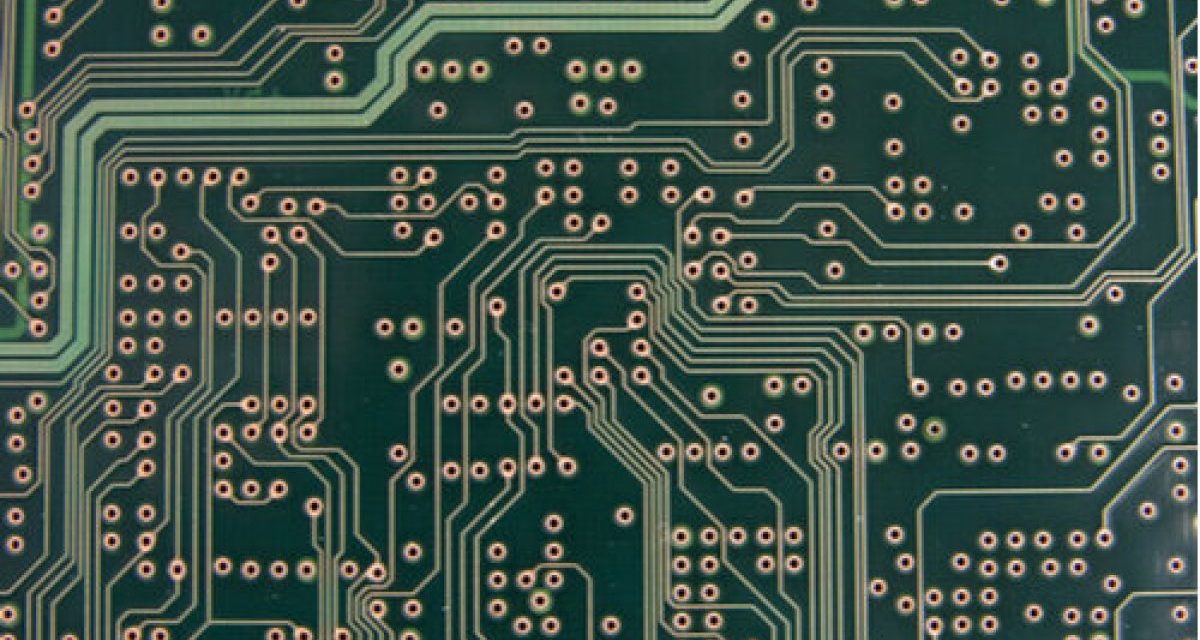
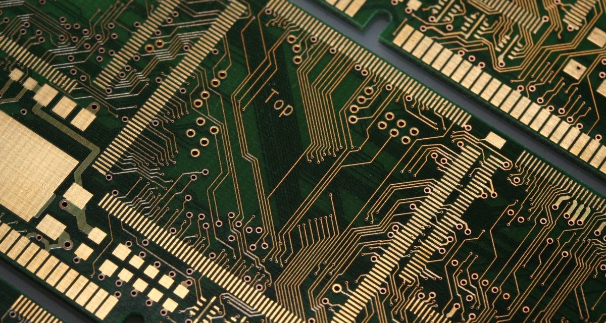
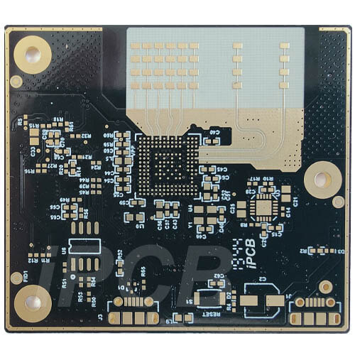
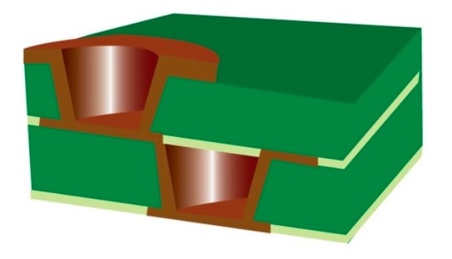
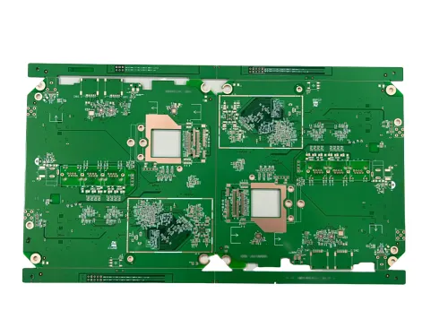
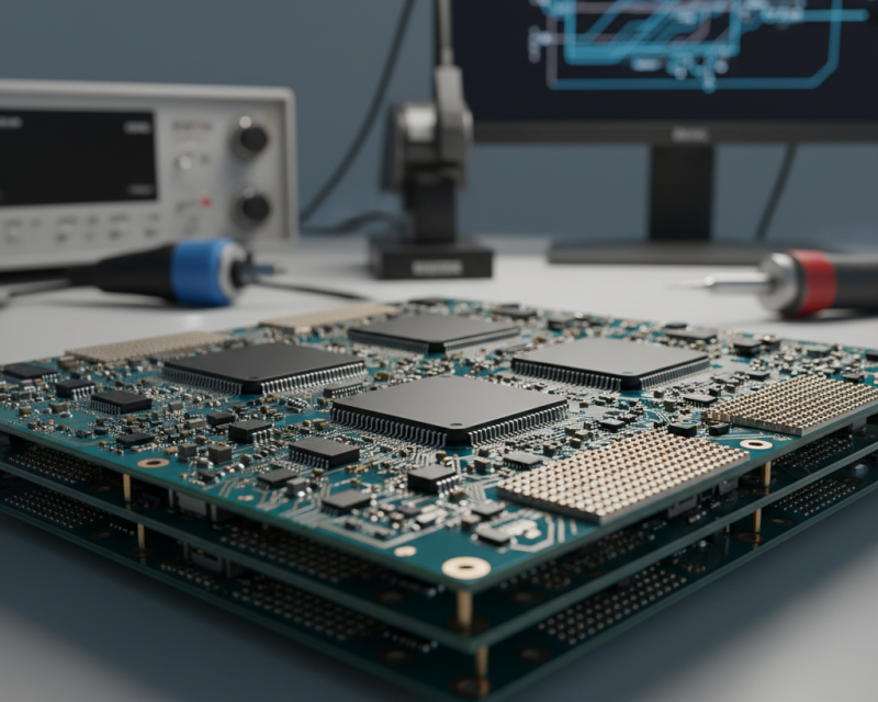
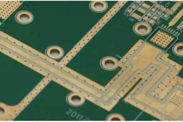
HDI PCB - KKPCB
 
HomeTag

HDI PCB - KKPCB

Blind and Buried Vias in PCB Design – Advanced HDI Interconnection Solutions

Blind and Buried Vias in PCB Design — Structure, Function, and Manufacturing Insights As the miniaturization of electronic components continues to accelerate, PCB designs must accommodate finer pitch components and higher circuit densities, especially in advanced mobile, communication, and computing applications. One of the critical technologies enabling this evolution is the use of blind and...

5G and IoT PCB Technology: How KKPCB Powers the Future of Intelligent Connectivity

5G and IoT: Transforming the World Through Intelligent Connectivity. 5G represents the fifth generation of wireless communication — not merely an upgrade from 4G, but a fundamental leap forward. With lightning-fast data transfer, ultra-low latency, and massive device connectivity, 5G unlocks the full potential of the Internet of Things (IoT). From smart cities to autonomous...

HDI PCB: The Core Technology Driving Miniaturization and High-Performance Electronics

HDI PCB: The Foundation of Modern Electronic Miniaturization In today’s electronics industry, devices are becoming smaller, faster, and more powerful. To achieve this balance, engineers increasingly rely on HDI PCBs (High-Density Interconnect Printed Circuit Boards)—a technology that allows for higher circuit density, improved signal integrity, and enhanced performance within compact form factors. At KKPCB, we...