fine-pitch PCB - KKPCB
 
HomeTag

fine-pitch PCB - KKPCB

Fine Line PCB: Advanced Manufacturing for High-Density & Miniaturized Circuit Designs

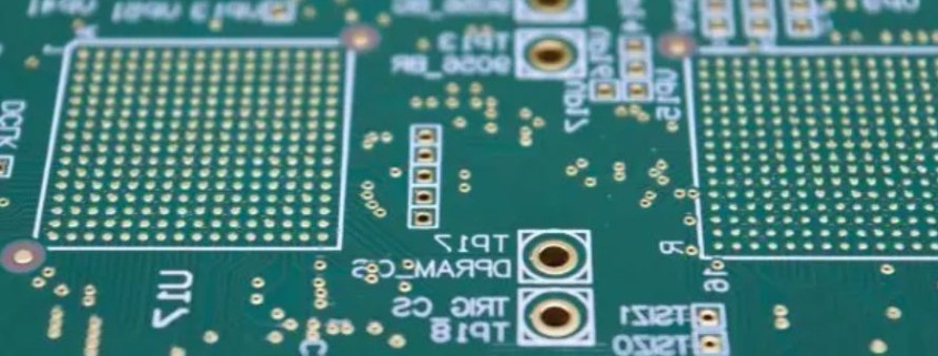
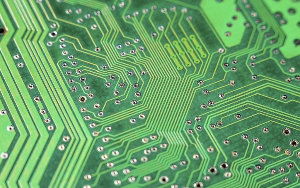
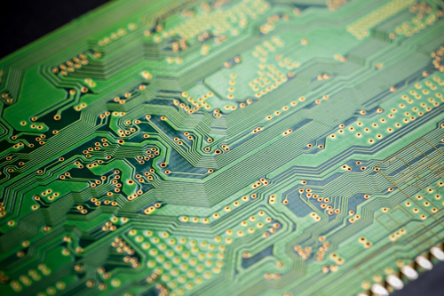
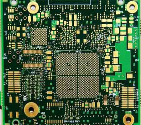
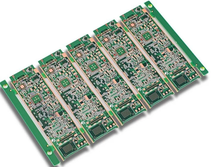
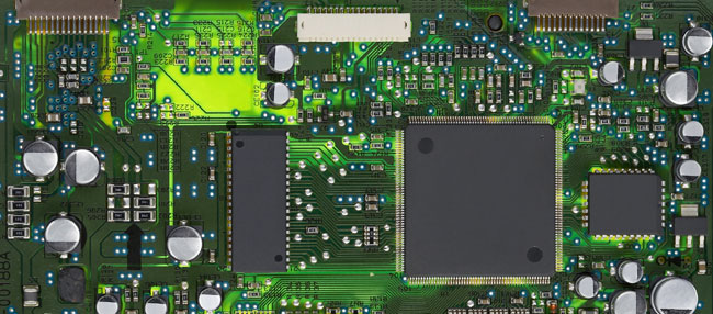
What is a Fine Line PCB? A Fine Line PCB refers to a printed circuit board with extremely narrow trace width and spacing, typically below 100 μm (4 mil) and often reaching 50 μm (2 mil) or less in advanced designs. These PCBs are essential for high-density interconnect (HDI) and miniaturized electronic products, where space...

HDI PCBs: High-Density Interconnect Solutions for Next-Generation Electronics

Why HDI PCBs Are No Longer Optional As electronic devices become smaller, faster, and more complex, traditional multilayer PCB designs struggle to keep up. HDI (High-Density Interconnect) PCBs address this challenge by enabling higher routing density, shorter signal paths, and better electrical performance. At the core of HDI technology is the use of: Microvias (laser-drilled...

Probe Card PCBs: Precision Platforms for Semiconductor Testing

What Makes Probe Card PCBs Unique A Probe Card PCB is not a typical circuit board—it is a high-precision interface platform used in semiconductor wafer testing. It connects test equipment (ATE) to microscopic pads on silicon wafers through probe needles or MEMS structures. Unlike standard PCBs, probe card boards must support: Ultra-fine pitch interconnections High...

BT Epoxy PCBs: High-Performance Solutions for Multi-Layer and High-Density Electronics

A BT Epoxy PCB is a printed circuit board that uses Bismaleimide-Triazine (BT) resin as the substrate material. BT Epoxy offers low coefficient of thermal expansion (CTE), high glass transition temperature (Tg), and excellent dimensional stability, making it ideal for multilayer, high-density, and fine-pitch applications. BT Epoxy PCBs are particularly suitable for: High-performance computing and...

Fine Pitch PCBs: Precision Design for High-Density Components

As electronic devices become smaller and more powerful, the demand for Fine Pitch PCBs—boards designed for components with extremely small pin spacing—has grown significantly. Fine pitch components, such as BGA, QFN, and CSP packages, require precise PCB design and manufacturing to ensure electrical connectivity, signal integrity, and long-term reliability. Design Considerations High-Density Layouts:Fine pitch PCBs...

Microvia PCB – Laser-Drilled HDI Technology for High-Density Interconnection

What Is a Microvia PCB A Microvia PCB is a high-density interconnect (HDI) printed circuit board that uses laser-drilled microvias to connect adjacent copper layers. Unlike traditional mechanical through-holes, microvias are extremely small and typically connect only one or two layers. Microvia technology enables higher routing density, improved electrical performance, and more compact electronic designs....

Fine Line PCB – Precision Micro-Trace Technology for High-Density Circuit Design

What Is a Fine Line PCB? A Fine Line PCB refers to a printed circuit board manufactured with extremely narrow trace widths and spacing. Compared with standard PCB designs, fine line technology enables higher routing density within limited board space. Fine line PCBs are essential for modern electronic devices where compact size, high functionality, and...

Microvia PCB – High Density Interconnect PCB for Advanced Electronic Applications

Microvia PCB for High Density Interconnect (HDI) Design As electronic products continue to shrink in size while increasing in functionality, traditional through-hole PCB structures are no longer sufficient. Microvia PCB technology enables higher routing density, improved signal integrity, and compact multilayer stackups, making it essential for modern high-performance electronics. Microvias are laser-drilled vias typically with...

Fine Pitch PCB – Precision PCB for High Density and Fine Line Applications

What Is Fine Pitch PCB? A Fine Pitch PCB refers to a printed circuit board designed with extremely small trace width and spacing to support high pin count and fine pitch components. It is commonly used in advanced electronic systems where compact design, high integration, and precise routing are essential. Fine pitch designs are typically...

HDI PCB – High Density Interconnect PCB for Advanced Electronics

What Is HDI PCB? HDI PCB (High Density Interconnect PCB) is a printed circuit board designed with higher wiring density per unit area compared to traditional multilayer PCBs. It uses advanced manufacturing technologies such as microvias, blind vias, buried vias, and fine line traces to achieve compact size and improved electrical performance. HDI PCB is...