EMI suppression - KKPCB
 
HomeTag

EMI suppression - KKPCB

Enhance Multi-Layer Impedance Control and Low-Loss Performance Using TLY-5 PCB for mmWave Communication Systems

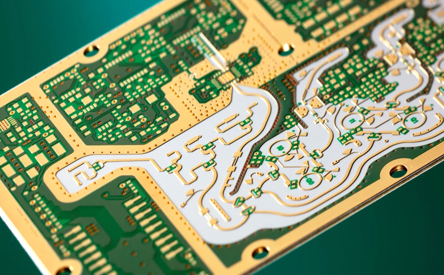
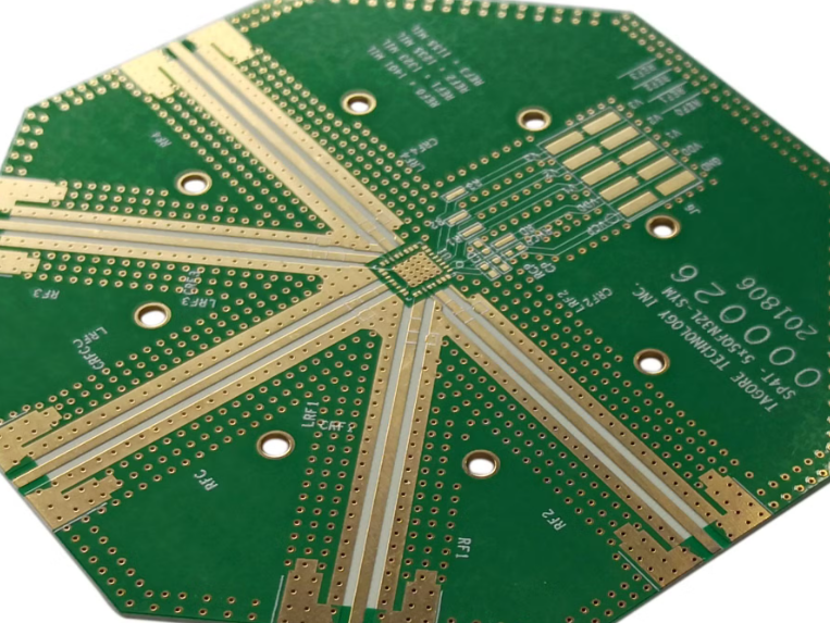
1. Engineering Context Next-generation mmWave communication systems—including 5G base stations, satellite payloads, and radar modules—require PCBs that provide ultra-stable impedance, low insertion loss, and phase-consistent routing. Traditional FR-4 or high-speed laminates often suffer from dielectric drift, higher Df, and thermal expansion issues, which degrade signal fidelity, EMI immunity, and system reliability in dense multi-layer RF...

Reduce Insertion Loss and Enhance Power Efficiency Using Low Loss PCB Designs for Satellite Communication Payloads

Satellite communication payloads demand high-frequency RF stability, minimal insertion loss, and optimized power efficiency across densely packed multilayer PCBs. Signal integrity degradation, EMI coupling, or thermal hotspots can compromise link margin, telemetry accuracy, and antenna performance. Low loss PCB materials, such as ceramic-reinforced laminates or PTFE-based RF substrates, provide stable dielectric constant (Dk) and low...

Optimize Phase-Stable High-Frequency Routing with Blind Via PCB Architectures in Compact Satellite Communication Payloads

Compact satellite communication payloads require precise, phase-stable RF routing to maintain signal fidelity and low insertion loss across high-frequency channels. The limited space and high-density requirements make blind via architectures essential for multilayer PCBs, enabling signal interconnects without penetrating all layers, reducing parasitic capacitance, and controlling crosstalk. Blind via PCBs allow compact routing of RF...

Minimize Crosstalk and Maintain Impedance Precision Using Advanced Blind Via PCB Layouts in 5G mmWave Systems

5G mmWave hardware doesn’t leave much room for layout mistakes. When operating above 24 GHz, a few microns of misalignment, a poorly shaped via stub, or an uncontrolled dielectric transition can collapse RF integrity. That is why advanced blind via PCB layouts have become a core enabling technology for minimizing crosstalk, stabilizing impedance, and preserving...

Unlock Ultra-Stable RF Propagation and Low-Loss Routing with Next-Gen Multilayer HF PCB Platforms for Dense mmWave Arrays

Dense mmWave arrays, commonly used in 5G massive MIMO, radar, and satellite phased arrays, require ultra-stable RF propagation, minimal insertion loss, and precise impedance control across multilayer interconnects. Thermal stress, mechanical vibration, and high-frequency crosstalk can severely degrade signal fidelity, phase alignment, and overall array performance. Next-generation multilayer HF PCB platforms leverage advanced dielectric laminates...

Improve Wideband Isolation and EMI Suppression Using Engineered 5G Router PCB Layouts for CPE Systems

Customer-Premises Equipment (CPE) sits at the frontline of the 5G access network. Unlike traditional routers, a 5G CPE must simultaneously maintain wideband RF isolation, suppress broadband EMI, and stabilize the 2.4 GHz / 5 GHz / 6 GHz multi-band wireless channels while handling dense digital switching activity. At these frequencies, the PCB layout is no...

Drive Ultra-Clean Electromagnetic Performance Through Precision-Aligned Multilayer HF PCB Dielectrics in Wideband Radar Processing Units

Wideband radar processing units operating in 8–40 GHz and beyond require multilayer HF PCBs with precisely aligned dielectric layers to maintain ultra-clean electromagnetic performance. Signal integrity, insertion loss, and phase stability are critically sensitive to stackup alignment, trace spacing, and dielectric uniformity. KKPCB leverages precision-laminated multilayer HF PCB substrates, low-roughness copper, and impedance-calibrated routing to...

Optimize RF Transmission and Phase Consistency Using High-Frequency Sensor PCB Laminates in Automotive ADAS Sensing Modules

Next-generation automotive ADAS sensing modules, including 77–81 GHz radar, LiDAR, and mmWave sensor arrays, require PCBs with ultra-stable dielectric properties, low insertion loss, and phase-coherent RF routing. Performance depends on maintaining consistent Dk/Df, low-loss mmWave signal propagation, and minimal EMI, even under harsh thermal cycling, vibration, and humidity conditions in vehicles.   High-frequency sensor PCB...

Enhance Signal Integrity and Thermal Reliability with ADAS PCB Platforms for Automotive Radar Systems

Advanced Driver Assistance Systems rely heavily on 77 GHz automotive radar modules, where the ADAS PCB directly determines signal integrity, insertion loss, dielectric stability, and system-level thermal reliability. As radar sensors expand from single-beam to multi-beam architectures, PCB materials and stackup selection have become primary constraints for RF linearity and long-distance object detection. The objective...

Impedance Control and RF Efficiency Optimization Using Ceramic PCBs in Industrial Wireless Sensor Networks

1. Engineering Overview / Abstract   As Industrial IoT communication modules become more compact and operate at higher frequencies, maintaining precise impedance control and RF efficiency is critical for reliable data transmission. Traditional polymer-based PCBs often suffer from dielectric drift, thermal warpage, and EMI coupling, which degrade signal integrity in dense wireless sensor networks.  Ceramic...