Controlled Impedance PCB - KKPCB
 
HomeTag

Controlled Impedance PCB - KKPCB

Enhance Routing Density and Signal Integrity with Buried Via PCB Architectures for High-Density Electronic Systems

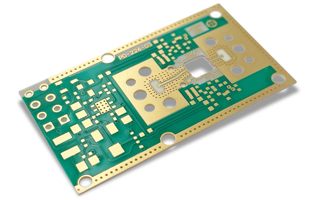
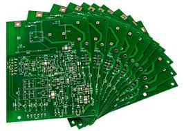
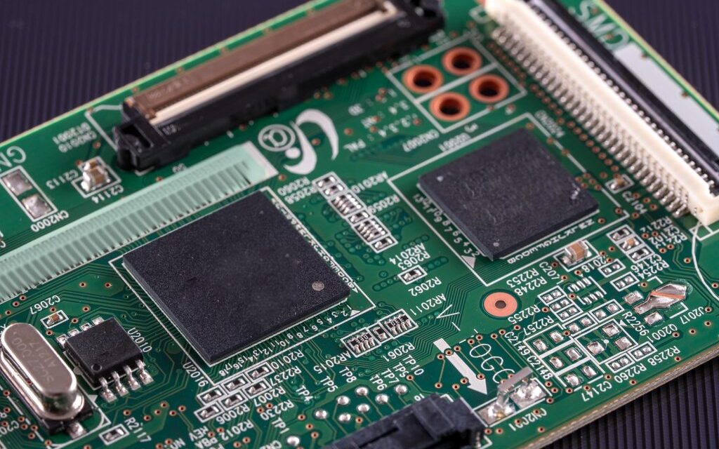
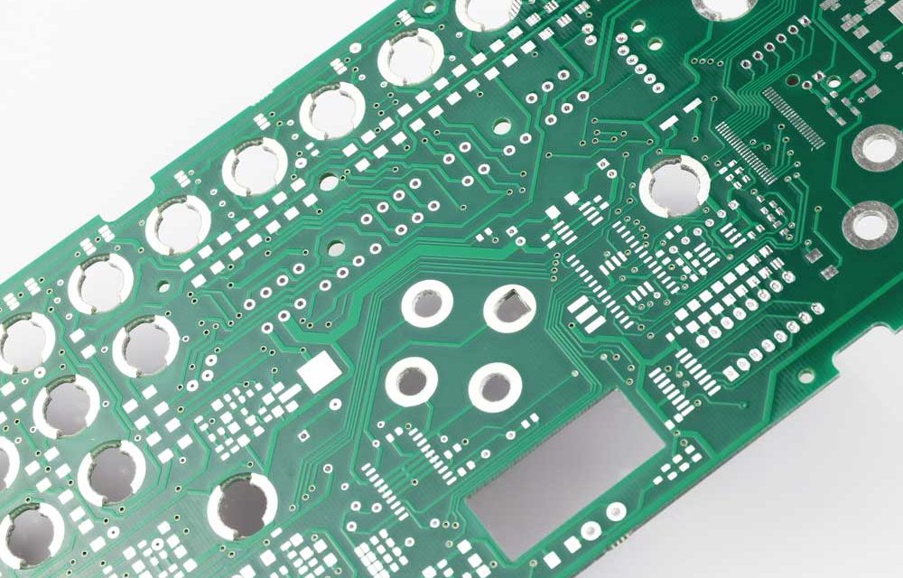
Buried Via PCB: Enabling High-Density Interconnection Beyond Conventional Multilayer Boards A Buried Via PCB is a multilayer printed circuit board in which vias connect only internal layers and do not extend to the outer layers. Unlike through-hole vias, buried vias are completely embedded within the PCB stackup, enabling higher routing density, improved signal integrity, and...

Enable Ultra-Complex Routing and Signal Integrity with High Layer Count PCB Architectures for Advanced Electronic Systems

High Layer Count PCB: The Backbone of Ultra-Complex Electronic Integration A High Layer Count PCB refers to a multilayer printed circuit board typically exceeding 12 layers and extending to 20, 30, or even 60+ layers for advanced electronic systems. High layer count PCB designs are essential for applications requiring dense routing, high-speed signal transmission, controlled...

Optimize High-Frequency Signal Integrity and Power Efficiency with Low Dissipation Factor PCB Materials

Why Low Dissipation Factor PCB Matters in High-Frequency Electronics As electronic systems evolve toward higher frequencies, faster data rates, and tighter power budgets, signal loss within the PCB itself becomes a dominant performance constraint. In RF, microwave, mmWave, high-speed digital, and satellite communication systems, even minor dielectric losses can accumulate across long signal paths, directly...

Improve Thermal Reliability and Signal Integrity with High TG PCB Materials for High-Performance Electronic Systems

Engineering Context: Why High TG PCB Is Critical in Modern Electronics As electronic systems continue to push toward higher power density, faster signal speeds, and harsher operating environments, conventional PCB materials increasingly become a reliability bottleneck. Excessive heat, repeated thermal cycling, and dense component placement place enormous stress on standard laminates, often leading to warpage,...

High-Stability Double Layer HF PCB Engineering for Low-Loss RF Routing and Precision High-Frequency Performance

A Double Layer HF PCB is one of the most efficient and cost-optimized architectures for high-frequency designs requiring low-loss transmission, tight impedance control, and stable RF performance up to microwave and lower mmWave ranges. Compared with complex multilayer structures, the Double Layer HF PCB offers a cleaner electromagnetic environment, reduced dielectric loading, and minimized stackup...

Engineering Double Layer HF PCB for Ultra-Stable RF Performance and Low-Loss Microwave Signal Integrity

As RF communication, IoT edge devices, automotive radar, and compact wireless modules continue to evolve, the Double Layer HF PCB has become a preferred architecture for delivering high-frequency stability, low insertion loss, and predictable electromagnetic performance. Although limited to two copper layers, a Double Layer HF PCB—when engineered correctly—can outperform many multilayer structures in signal...

Unleash Multi-Gigabit Data Fidelity with Precision-Engineered High Speed PCB Architectures for Next-Gen Digital Systems

A High Speed PCB forms the electrical backbone of every modern digital communication system, from multi-gigabit SerDes channels to DDR memory interfaces and high-frequency RF-digital mixed platforms. As data rates continue pushing beyond 10 Gbps, 25 Gbps, and even 56–112 Gbps PAM-4, the engineering demands on a High Speed PCB become far more stringent. Signal...

Advanced TLY-5 PCB Technologies for Low-Loss, High-Stability RF and mmWave Communication Systems

TLY-5 PCB materials have become a core enabler in modern high-frequency electronics, especially as RF, microwave, and mmWave systems continue pushing toward higher bandwidth, lower loss, and stricter phase-stability requirements. Built on a PTFE-based low-loss dielectric platform, TLY-5 PCBs deliver exceptionally high electrical performance while supporting the reliability demands of satellite payloads, radar front-ends, high-power...

Boost Design Accuracy and Signal Integrity Using High-Precision PCB Prototype Fabrication Technologies

High-precision PCB prototype fabrication has become the backbone of modern electronics development. As product cycles shrink and system complexity rises—spanning RF modules, high-speed digital interfaces, IoT sensors, EV power systems, and aerospace electronics—the demand for PCB prototype accuracy, signal integrity stability, and manufacturing predictability has never been higher. A high-reliability prototype is not “just a...

Optimize Low-Loss Signal Chains and EMI Control Using RF Transceiver PCB Designs for High-Frequency Communication Systems

High-frequency communication systems—from 5G NR radios and phased-array front ends to satellite downlink modules and wideband radar—rely on precisely engineered RF Transceiver PCB architectures to maintain low-loss signal chains, stable phase performance, and strong EMI suppression. As operating frequencies rise into sub-6 GHz, C-band, Ku-band, Ka-band and even mmWave ranges, the electrical behavior of the...