Buried Via PCB - KKPCB
 
HomeTag

Buried Via PCB - KKPCB

HDI PCB – High Density Interconnect PCB for Advanced Electronics

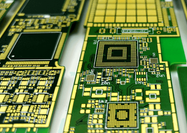
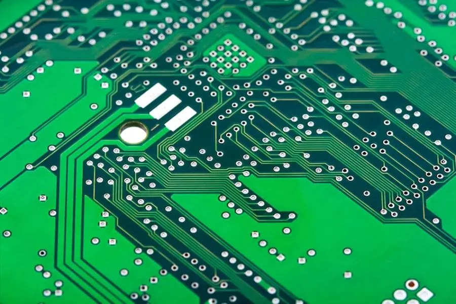
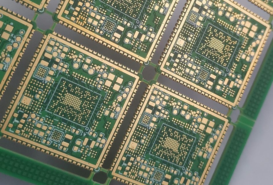
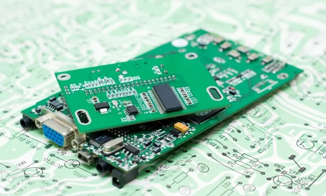
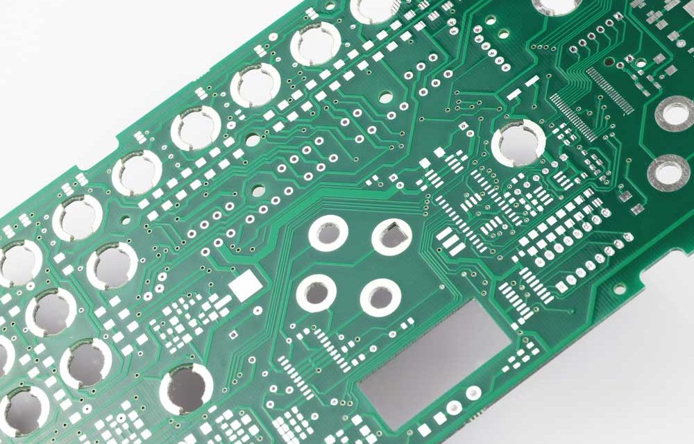
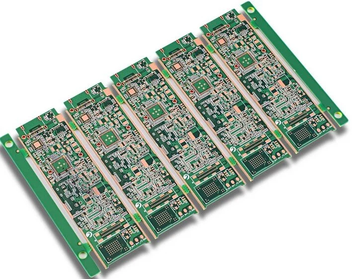
What Is HDI PCB? HDI PCB (High Density Interconnect PCB) is a printed circuit board designed with higher wiring density per unit area compared to traditional multilayer PCBs. It uses advanced manufacturing technologies such as microvias, blind vias, buried vias, and fine line traces to achieve compact size and improved electrical performance. HDI PCB is...

Buried Via PCB – Advanced Multilayer PCB with Internal Interconnection Technology

What Is a Buried Via PCB? A Buried Via PCB is a multilayer printed circuit board that contains vias connecting internal layers only, without reaching the outer surface layers. Unlike through-hole vias, buried vias are completely enclosed within the board stack-up. This allows designers to: Increase routing density Optimize outer layer space Improve signal integrity...

Buried Via PCB for High-Density and Advanced Multilayer Circuit Designs

What Is a Buried Via PCB? A Buried Via PCB is a multilayer printed circuit board that uses vias connecting only internal layers without reaching the outer surface layers. These hidden interconnections allow designers to increase routing density while maintaining surface space for components and signal traces. Buried Via PCBs are widely used in HDI...

High Density PCB: Advanced Solutions for Compact and High-Performance Electronics

A High Density PCB (HDPCB) is a printed circuit board designed to support compact, high-performance electronic systems. By leveraging HDI technology, microvias, blind/buried vias, and multilayer stackups, high density PCBs allow engineers to integrate more functionality into smaller footprints, making them essential for smart devices, high-speed computing, RF communication, and semiconductor testing. Key Features of...

Designing Buried Via PCBs for High-Density Routing and Signal Integrity Optimization

As electronic systems continue to evolve toward higher speed, smaller form factors, and increased functionality, traditional through-hole via structures are becoming a limiting factor. Buried Via PCB technology has emerged as a critical enabler for high-density routing and signal integrity optimization, particularly in HDI, high-speed digital, and RF applications. By embedding vias between inner layers...

Balancing Electrical Performance and Manufacturability in Buried Via PCB Structures

As electronic systems continue to evolve toward higher speeds, greater functionality, and reduced form factors, Buried Via PCB structures have become a critical enabler for advanced multilayer designs. By allowing interlayer connections without penetrating the outer layers, buried vias unlock higher routing density, improved signal integrity, and enhanced EMI control. However, these electrical advantages must...

Enhance Routing Density and Signal Integrity with Buried Via PCB Architectures for High-Density Electronic Systems

Buried Via PCB: Enabling High-Density Interconnection Beyond Conventional Multilayer Boards A Buried Via PCB is a multilayer printed circuit board in which vias connect only internal layers and do not extend to the outer layers. Unlike through-hole vias, buried vias are completely embedded within the PCB stackup, enabling higher routing density, improved signal integrity, and...