BGA footprint design - KKPCB
 
HomeTag

BGA footprint design - KKPCB

BGA Assembly: Beginner’s Guide to Ball Grid Array Assembly

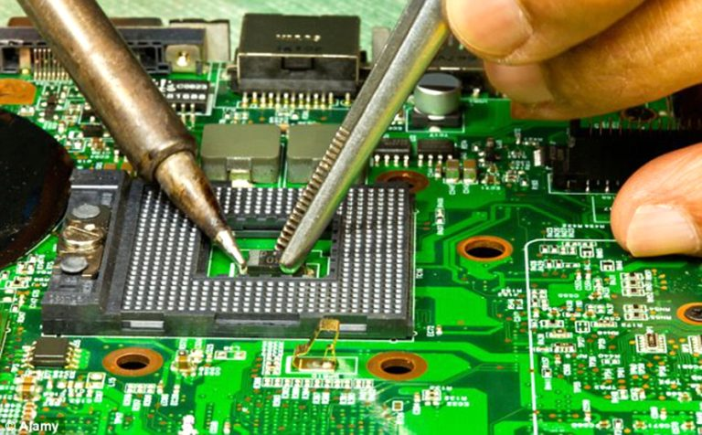
Why BGA Assembly Is Critical in Modern PCB Design As electronic devices move toward miniaturization, high-speed performance, and high pin-count integration, the Ball Grid Array (BGA) assembly has become a mainstream packaging technology in: Microprocessors (CPU/GPU) FPGAs High-speed communication ICs Memory devices (DDR, LPDDR) Compared with traditional packages (QFP, SOP), BGA offers: Higher I/O density...

Advanced PCB Footprint Generator: Key to Efficient PCB Design

Why PCB Footprint Accuracy Matters In modern high-speed PCB design, HDI PCB development, and high-density electronic systems, the accuracy of PCB footprints (land patterns) directly impacts: Assembly yield Solder joint reliability Manufacturing efficiency Time-to-market A poorly designed footprint can result in: Component misalignment Solder bridging or tombstoning Rework and production delays This is why advanced...