Back Drilling PCB - KKPCB
 
HomeTag

Back Drilling PCB - KKPCB

Load Board PCB – High Precision Interface Board for Semiconductor Testing

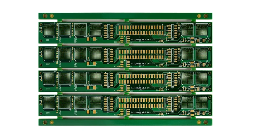
What Is a Load Board PCB? A Load Board PCB is a critical interface board used in Automated Test Equipment (ATE) systems for semiconductor device testing. It connects the tester to the device under test (DUT), transmitting signals, power, and measurement data with high accuracy and stability. Load boards are specifically engineered to support high...

High Layer Count PCB – Advanced Multilayer PCB for High Density and High Speed Applications

What Is a High Layer Count PCB? A High Layer Count PCB refers to a multilayer printed circuit board typically built with 16 layers or more, and in advanced applications, up to 40, 60, or even higher layer counts. High Layer Count PCB is designed to support: High density routing Complex signal distribution Controlled impedance...