Electronics Industry NewsEngineering TechnologiesPCB Assembly (PCBA)PCB DesignPCB ManufacturingPCB Materials
Semiconductor Load Board: High-Performance PCBs for Accurate ATE IC Testing
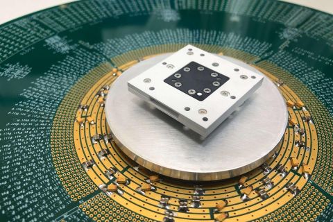
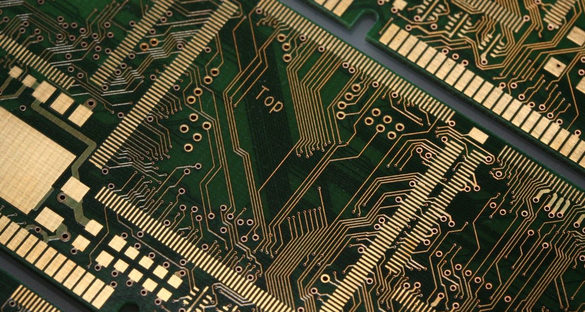
A Semiconductor Load Board is a specialized ATE test PCB that serves as the electrical interface between Automated Test Equipment (ATE) and the device under test (DUT). Load boards route signals, power, and control lines from the tester to the IC through test sockets, enabling precise functional and parametric testing during semiconductor validation and mass...