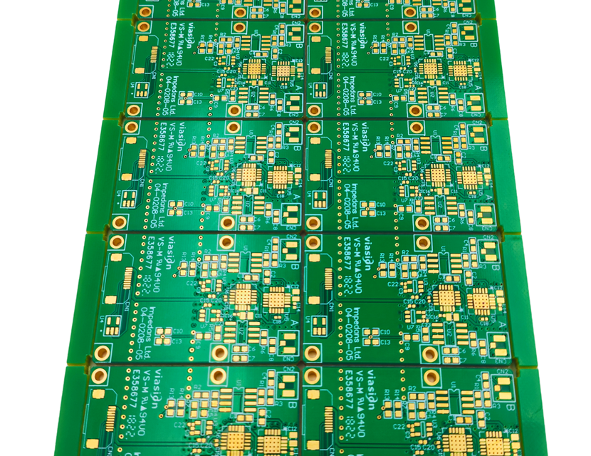
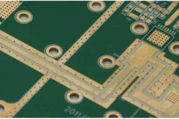
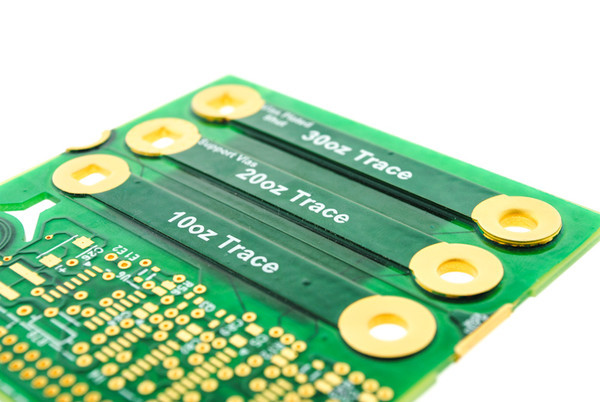
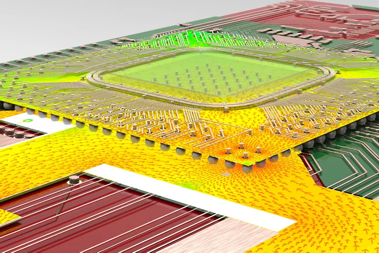
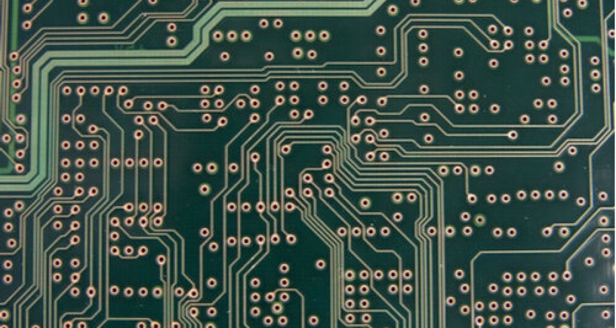
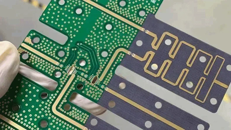
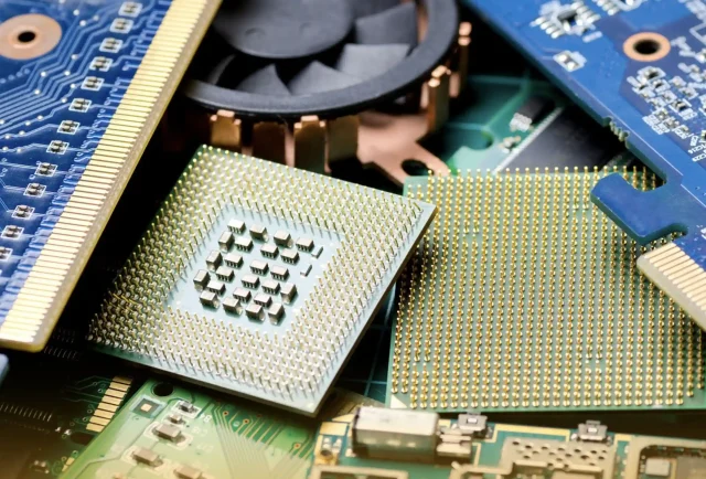
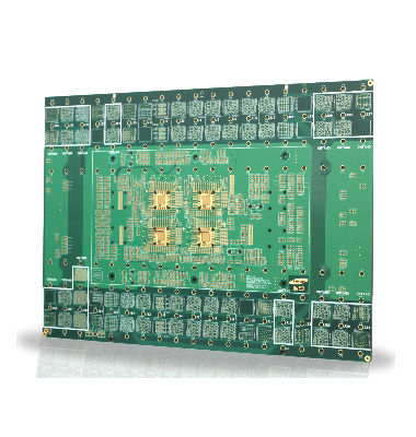
Advanced Engineering Technologies for PCB & PCBA Solutions - KKPCB
 
HomeCategory

Advanced Engineering Technologies for PCB & PCBA Solutions - KKPCB

Order Microwave PCB: What to Know for High-Performance Microwave and RF Applications

When you order microwave PCB solutions for advanced electronic systems, precision, material performance, and manufacturing expertise are critical. Microwave PCBs operate at extremely high frequencies, where signal loss, impedance mismatch, and dielectric instability can severely impact overall system performance. This article explains the key factors to consider when ordering microwave PCBs, helping engineers and purchasing...

Purchase RF PCB: Key Considerations for Reliable High-Frequency and Microwave Applications

When you purchase RF PCB solutions for high-frequency and microwave applications, performance, reliability, and manufacturing precision are critical. RF PCBs are widely used in wireless communication, radar systems, satellite electronics, and RF front-end modules, where even small design or process deviations can significantly impact signal quality. This article explains what to consider when purchasing RF...

Buy High Frequency PCBs Using Rogers, PTFE, and Hybrid Stackups for High-Speed RF Front-End Modules

As wireless communication, radar systems, and high-speed data transmission continue to advance, high frequency PCBs have become a critical foundation for modern RF front-end modules. Selecting the right materials and stack-up structures—such as Rogers PCBs, PTFE PCBs, and hybrid PCB stackups—is essential to achieving low loss, stable impedance, and reliable RF performance. This article explains...

Accelerate Product Validation and Engineering Iteration with High-Reliability Small Batch PCB Manufacturing

In today’s highly competitive electronics market, speed and reliability are critical during the product development stage. High-reliability small batch PCB manufacturing enables engineers to accelerate product validation, shorten engineering iteration cycles, and reduce development risk before mass production. This article explains how small batch PCB manufacturing supports rapid prototyping, design verification, and engineering optimization, helping...

PCB Turnkey Services: A Complete One-Stop Solution for PCB Manufacturing and Assembly

PCB Turnkey Services: A Complete One-Stop Solution for PCB Manufacturing and Assembly In today’s fast-paced electronics industry, reducing supply chain complexity and accelerating time to market are critical for success. PCB Turnkey services provide a complete, one-stop solution that covers every stage of electronics production—from PCB fabrication and component sourcing to assembly, testing, and final...

Impedance Control on PCBs: Why It Matters for High-Speed, RF, and High-Frequency Circuit Design

As electronic devices continue to evolve toward higher speeds, greater bandwidth, and higher operating frequencies, impedance control on PCBs has become a critical requirement rather than an optional design consideration. In high-speed PCB, RF PCB, and high-frequency circuit design, improper impedance control can lead to signal degradation, EMI issues, and overall system instability. This article...

Key Manufacturing Factors That Affect Controlled Impedance PCB Accuracy

Key Manufacturing Factors That Affect Controlled Impedance PCB Accuracy In today’s high-speed electronics market, Controlled Impedance PCB manufacturing has become a fundamental requirement for ensuring excellent signal integrity and stable electrical performance. As operating frequencies and data transmission speeds continue to rise, even minor impedance deviations in a controlled impedance PCB can result in signal...

Buy High Frequency PCBs Optimized for Controlled Impedance and Low Insertion Loss in 5G and Satellite Systems

As 5G wireless infrastructure and satellite communication systems continue to evolve toward higher frequencies, wider bandwidths, and denser integration, the demand to buy high frequency PCBs with precise electrical control has increased significantly. In these applications, controlled impedance PCB design and ultra-low insertion loss PCB performance are no longer optional—they are fundamental to achieving stable...

Designing Buried Via PCBs for High-Density Routing and Signal Integrity Optimization

As electronic systems continue to evolve toward higher speed, smaller form factors, and increased functionality, traditional through-hole via structures are becoming a limiting factor. Buried Via PCB technology has emerged as a critical enabler for high-density routing and signal integrity optimization, particularly in HDI, high-speed digital, and RF applications. By embedding vias between inner layers...

Small Batch PCB Manufacturing: Enabling Flexible Engineering Validation and Low-Risk Product Development

Why Small Batch PCB Matters in Modern Electronics Development In today’s electronics industry, product lifecycles are shorter and design iterations are more frequent. Before committing to mass production, engineering teams must validate signal integrity, power stability, thermal behavior, and manufacturability. Small batch PCB manufacturing plays a critical role in this phase by enabling controlled, low-risk...