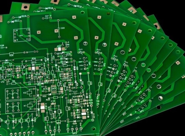
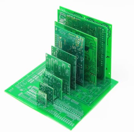
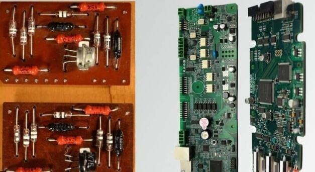
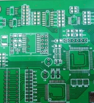
kkpcba-Cindy - KKPCB - Page 43 of 73
 
HomeAuthor

kkpcba-Cindy - KKPCB - Page 43 of 73

How to Overcome Challenges in PCB Copy Board Design in the Intelligent Era

With the advancement of policies by the National People’s Congress and the Chinese People’s Political Consultative Conference supporting entrepreneurship and innovation, the electronics industry has been rapidly transforming, propelling us into the intelligent era. In this context, upgrading PCB copy board design technology has become essential. With the expansion of the smartphone and tablet markets,...

Enhancing Anti-Static ESD Function in PCB Design

In PCB design, effective ESD (Electrostatic Discharge) protection can be achieved through strategic layering, layout, and installation adjustments. ESD protection aims to shield delicate semiconductor chips from static electricity originating from humans, the environment, or even other electronic components, which can damage insulation layers, MOSFET and CMOS gates, PN junctions, and wiring. Here are some recommended techniques...

PCB Design Principles for Single-Chip Microcontroller Control Boards

Effective PCB design for single-chip microcontroller (MCU) control boards involves structured layout and routing principles to minimize interference and enhance performance. Proper planning of input/output paths, decoupling, grounding, and component placement is crucial. 1. Component Layout for Reduced Interference Proximity Placement: Place related components, especially noise-sensitive ones (e.g., clock inputs, crystal oscillators, CPU), as close together as possible....

Electromagnetic Compatibility (EMC) Challenges in PCB Design

With rising PCB trace speeds, electromagnetic compatibility (EMC) becomes increasingly crucial in PCB design. Key EMC attributes are essential to analyze in order to identify and mitigate potential interference sources. Below are the five critical attributes to consider during EMC analysis, followed by practical layout strategies. 1. Key Component Size and Trace Length Radiating Device Size: The...

PCB Design Wiring Rules: Best Practices for Optimal Performance

Wiring in PCB design is a critical step that directly impacts product performance. With the complexities of single-sided, double-sided, and multi-layer wiring, and methods like automatic and interactive wiring, designers must carefully consider routing techniques. Below, we outline essential PCB wiring rules and guidelines for achieving effective signal integrity, power management, and ground control. 1. Key Wiring Rules...

Essential Checkpoints for Final Stages of PCB Design

Inexperienced PCB designers often overlook critical checks in the later design stages, leading to issues like inadequate line width, misplaced silkscreens, and insufficient spacing near sockets. These errors can cause electrical or manufacturing issues, potentially requiring redesigns and increasing production costs. Below is a comprehensive list of essential PCB design checkpoints to ensure product quality and manufacturability....

How to Reduce Circuit Board Noise

In PCB design, a well-designed circuit can still produce noise during testing, leading to performance issues or even requiring a board redesign. Below, we explore strategies to reduce circuit board noise effectively. Functional Module Separation A high-performance board will often have a clear layout of functional modules. A functional module is a collection of circuits and components dedicated...

Precautions for PCB Design

In PCB design, circuit layout is fundamental for engineers. However, even experienced engineers may overlook critical details in basic PCB design, which can lead to errors. Sometimes, these errors may cause problems or even a complete failure of the circuit when converted into a PCB. To help engineers avoid redesigns and improve work efficiency, here are...

Grounding Methods for Multi-Layer PCB Boards

Grounding Method for Multi-Layer PCB Boards (I) Four-layer PCBs are typically used for high-density, high-frequency applications and offer more than 20 dB better electromagnetic compatibility (EMC) compared to two-layer boards. In a four-layer board setup, a complete ground plane and a full power plane can be used. This allows the various circuit ground wires to be connected...