Learn how skip vias improve HDI PCB design by reducing via stacks, lowering manufacturing costs, and enhancing reliability. Explore best practices, DFM rules, and applications in high-density PCBs.
Fabrication capacity for high density PCBs and packaging is currently increasing, especially in North America and Europe. These platforms still use standard via styles, namely through-hole vias, blind and buried vias, and core vias in HDI PCBs. But the electronics assembly and packaging world is no stranger to innovation, and there are alternative via options...
Many times we discuss complex boards with unique features and sensitive routing on this blog. But the reality is that most PCBs that are mass manufactured have lower layer counts and less complexity. 2-layer PCBs will continue to be high-volume products, and they are almost always the starting point for a new designer learning about PCB layout. In...
4-layer PCBs are the workhorses of many low-density digital and RF PCBs that still require some controlled impedance routing. 4-layer boards are also very useful for diverse power connections, and they can be used in power electronics that require many varied components and power levels. As soon as a 2-layer board becomes too dense, ground planes get...
PCBs operating at high power also tend to operate at high temperature, sometimes cycling between high and low temperatures repeatedly. Sometimes, a PCB will operate in a high ambient temperature environment, and the board needs to remove heat from components to prevent even higher temperatures from being reached in the system. Active cooling measures are...
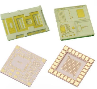
A ceramic substrate is an insulating material that provides a stable and rigid platform for mounting electronic components and creating electrical circuits. Ceramic substrates are often used as an alternative to epoxy-based materials like FR-4 (Flame Retardant 4). FR-4 is a popular substrate material for PCBs, but ceramic substrates offer certain advantages in specific applications. Key Characteristics...
Explore KKPCB’s 77GHz Millimeter Wave Radar PCB made with Rogers RO4835 + FR4 hybrid material. Engineered for automotive radar, ADAS, and 5G applications, this high-frequency PCB offers ultra-low loss, stable dielectric performance, and superior reliability. Ideal for 77GHz radar antennas, collision avoidance systems, and vehicle sensor modules requiring precision signal integrity and long-term stability.
In the fast-evolving world of high-frequency electronics, selecting the right PCB material is essential for achieving the performance required in modern applications such as automotive radar, wireless communication systems, and advanced microwave technology. The Rogers RO4835 + IT180 hybrid PCB, combining high-performance materials from Rogers, has emerged as a robust solution that delivers superior performance in these demanding fields....
PCB edge plating is a specialized process that involves applying a metal coating to the exposed copper connections at the edge of a printed circuit board (PCB). This technique, also known as side plating, battlement, or metallized edge plating, enhances electrical connectivity, structural rigidity, and electromagnetic interference (EMI) shielding. This article provides an in-depth look at the...
When designing for PCB prototyping, the cost of individual parts does not always play a big role. If you’re designing one-offs or hobby projects, you’ll probably only look at parts prices when your assembly house sends you an invoice. But if you’re eventually going to produce at scale, the cost of the prototype is small compared...