Wafer Test PCB - KKPCB
 
HomeTag

Wafer Test PCB - KKPCB

Semiconductor Test PCB: The Foundation of Accurate and Repeatable IC Testing

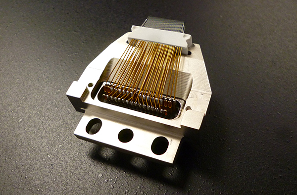
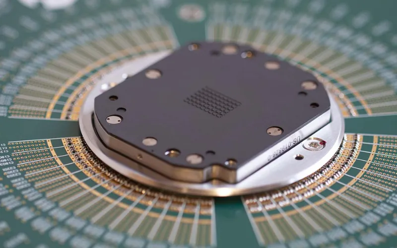
In semiconductor manufacturing, test accuracy directly affects yield, reliability, and time-to-market. Whether during engineering validation or high-volume production, the semiconductor test PCB serves as the critical electrical interface between automated test equipment (ATE) and the device under test (DUT). A professionally engineered semiconductor test PCB ensures stable measurements, consistent signal behavior, and long-term test reliability...

Probe Card PCB: Enabling High-Pin-Count and High-Speed Wafer-Level Testing

As semiconductor devices continue to scale down while pin counts and test speeds increase, wafer-level testing has become more demanding than ever. At the center of this process is the probe card PCB, a precision-engineered substrate that ensures accurate electrical connection between automated test equipment (ATE) and semiconductor wafers. A well-designed probe card PCB is...

Probe Card PCB: High-Precision Substrates for Advanced Semiconductor Testing

As semiconductor devices continue to scale in complexity and pin density, wafer-level testing requires extreme accuracy and repeatability. At the core of this process lies the probe card PCB, a critical interface that connects automated test equipment (ATE) to semiconductor wafers. A high-quality probe card PCB directly determines signal integrity, contact accuracy, and long-term test...