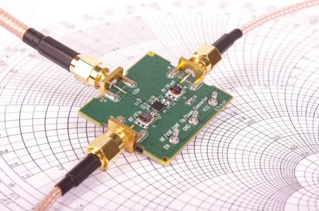
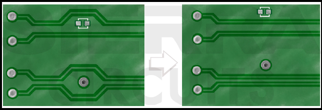
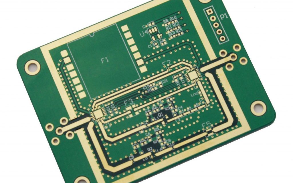
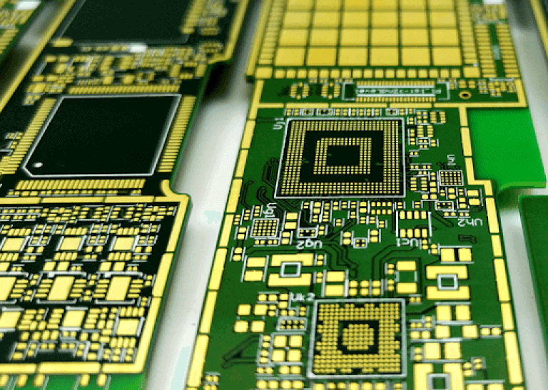
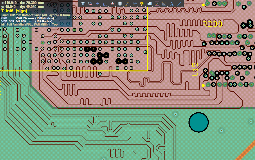
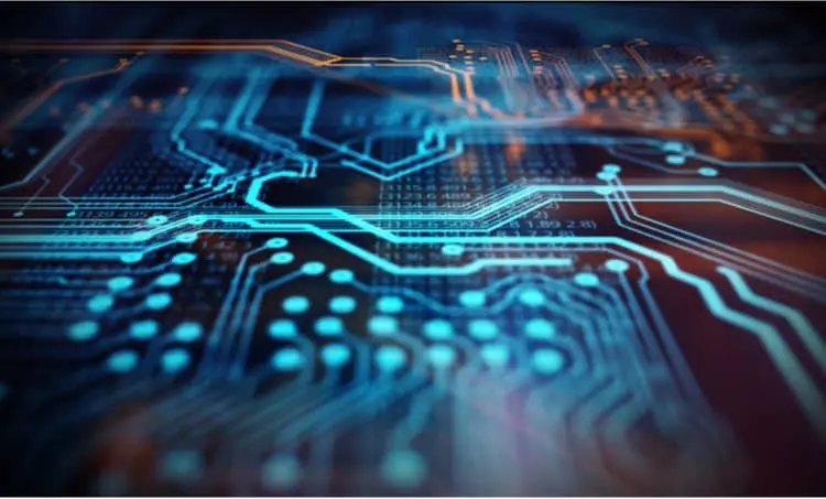
Signal Integrity - KKPCB
 
HomeTag

Signal Integrity - KKPCB

Shorten R&D Cycles with Cost-Optimized, High-Reliability PCB Prototype Solutions for Rapid Electronics Development

Rapid electronics development has entered an era where design cycles are measured not in months but in weeks. From IoT edge devices to next-generation communication modules and automotive sensing platforms, engineers must iterate faster while maintaining electrical performance, manufacturability, and long-term reliability. PCB prototypes sit at the heart of this acceleration. When engineered correctly, they...

Enhance Signal Accuracy and Low-Noise Stability with High Frequency Sensor PCB Platforms for Industrial IoT Detection Systems

Industrial IoT detection systems rely on a dense network of sensors for accurate monitoring of environmental parameters, machinery status, and process analytics. High frequency sensor PCBs must maintain low insertion loss, high signal-to-noise ratio, and phase-stable routing across multiple sensor channels to ensure reliable data acquisition. High frequency sensor PCB laminates (Dk = 3.2 ±...

Maximize RF Channel Integrity and Minimize Signal Loss with Blind Via PCB Architectures for High-Speed Communication Modules

High-speed communication modules in 5G, satellite transceivers, and high-frequency computing systems demand extreme precision in signal routing and interconnect integrity. As layer density increases and modules become more compact, traditional through-hole vias introduce unwanted parasitic effects, signal reflection, and EMI interference, compromising both channel fidelity and system performance. Blind via PCB technology enables selective inter-layer...

Optimize Signal Integrity and Multi-Band RF Stability with 5G Router PCB Architectures Using Low-Loss Materials

Next-generation 5G routers operate across 2.4, 5, and 6 GHz bands while supporting high-speed MIMO data streams and concurrent RF channels. Maintaining signal integrity, low insertion loss, and impedance accuracy across multilayer PCB architectures is critical for throughput, link stability, and network reliability. Low-loss PCB laminates (Dk ~3.0 ±0.04, Df ~0.0012 @10 GHz) provide minimal...

Achieve High-Frequency Channel Reliability and Precision Impedance Control with Megtron 7 PCB Stackups in Advanced Server Motherboards

Modern high-performance server motherboards handle multi-gigabit data streams across PCIe Gen5/Gen6, DDR5 memory, and high-speed interconnects. Ensuring channel reliability, minimal signal attenuation, and precise impedance control is critical to maintain data integrity, low bit error rates (BER), and thermal stability in dense server environments. Megtron 7 PCB laminates (Dk = 3.4 ± 0.03, Df =...

Enhance Signal Integrity and High-Speed Stability with Impedance Controlled PCB Platforms for 5G Communication Systems

5G communication systems rely on stringent impedance accuracy, low insertion loss, and predictable phase stability to maintain signal integrity across multi-gigabit transmission channels. At mmWave and sub-6 GHz bands, even slight deviations in controlled impedance routing can introduce reflection, jitter accumulation, and eye-diagram degradation.Impedance Controlled PCBs engineered for 5G must balance dielectric uniformity, copper surface...

Enhance Signal Integrity and Power Density with RO4350B PCB Designs in 5G Smartphone RF Front-Ends

RO4350B PCB materials are widely deployed in 5G smartphone RF front-end modules because they provide a balanced dielectric profile, low-loss characteristics, and stable RF transmission up to sub-6 GHz and selected mmWave bands. Modern antenna arrays, PA/LPF modules, LNA chains, and tunable impedance networks face stringent constraints in signal integrity, power density, EMI coupling, and...

High-Frequency Signal Integrity Optimization and Phase-Stable Transmission with Megtron 7 PCB Substrates in 5G Server and High-Speed Computing Systems

Megtron 7 PCB laminates are widely adopted in 5G servers, AI computing accelerators, and cloud networking equipment due to their exceptionally low dielectric loss and superior stability at 28–112 Gbps PAM4 and mmWave bands. As system architectures transition toward high-density multi-lane SerDes and advanced RF interconnects, PCB materials become a primary constraint influencing channel loss...

Hybrid Stackup and Miniaturized RF Design with PTFE PCBs in Next-Generation 5G Base Stations

1. Engineering Overview   Next-generation 5G base stations require high-density, miniaturized RF front-end modules with low insertion loss, precise impedance, and stable phase performance across mmWave bands (28–39 GHz).   PTFE PCB laminates, with Dk = 2.15 ± 0.02 and Df = 0.0009 @10GHz, provide superior dielectric consistency and thermal stability for tightly packed MIMO...

Dielectric Uniformity and Manufacturing Precision of PTFE PCBs for Aerospace Communication Equipment

1. Engineering Overview   Modern aerospace RF communication equipment, including satellite transceivers and spaceborne antenna modules, demands ultra-low-loss PTFE PCBs with tight dielectric uniformity and precise manufacturing tolerances. Small variations in Dk or CTE can lead to phase drift, impedance mismatch, and degraded link margin in Ku/Ka-band RF payloads.   PTFE PCB laminates, with Dk...