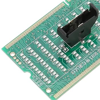
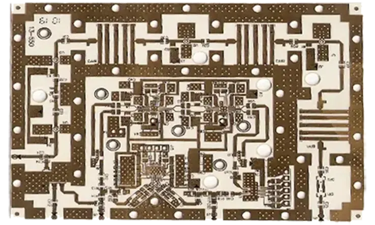
semiconductor test PCB - KKPCB
 
HomeTag

semiconductor test PCB - KKPCB

Fine Pitch PCB: Precision Solutions for High Pin Count and Miniaturized Electronics

A Fine Pitch PCB is a printed circuit board designed to support high-density integrated circuits with extremely small pad spacing, such as BGA, QFN, CSP, and flip-chip packages. As modern electronics continue to shrink in size while increasing functionality, fine pitch PCB technology becomes essential for achieving high routing density, reliable assembly, and superior electrical...

High Density PCB: Advanced Solutions for Compact and High-Performance Electronics

A High Density PCB (HDPCB) is a printed circuit board designed to support compact, high-performance electronic systems. By leveraging HDI technology, microvias, blind/buried vias, and multilayer stackups, high density PCBs allow engineers to integrate more functionality into smaller footprints, making them essential for smart devices, high-speed computing, RF communication, and semiconductor testing. Key Features of...

IoT IC Test PCB Solutions for Reliable and Scalable Smart Device Validation

An IoT IC Test PCB is a purpose-built printed circuit board designed to support functional testing, performance validation, and reliability verification of IoT integrated circuits. As IoT devices integrate wireless communication, low-power processing, sensors, and mixed-signal interfaces, the IoT IC test PCB plays a critical role in ensuring device accuracy, stability, and mass-production readiness. Key...

High Reliability PCB Manufacturing for Mission-Critical and Industrial Applications

What Is a High Reliability PCB? A High Reliability PCB is engineered to deliver stable electrical performance, mechanical durability, and long-term consistency under extreme operating conditions. Unlike standard commercial PCBs, high reliability PCBs are designed to withstand high temperature, thermal cycling, vibration, humidity, and continuous operation without performance degradation. These boards are widely used in...

Multilayer PCB: Enabling High-Density, High-Speed, and Complex Electronic Systems

A Multilayer PCB is a printed circuit board composed of three or more conductive copper layers laminated together with insulating materials. As electronic products continue to demand higher functionality, faster signal speeds, and smaller form factors, multilayer PCBs have become the backbone of advanced electronics, semiconductor testing, communication systems, and industrial control equipment. Compared with...

Low Loss PCB: High-Performance Solutions for High-Speed and High-Frequency Electronics

A Low Loss PCB is a specialized printed circuit board designed to minimize signal attenuation, dielectric loss, and insertion loss in high-speed digital and high-frequency RF applications. As modern electronics operate at multi-GHz frequencies and multi-gigabit data rates, signal loss caused by PCB materials and structures becomes a critical limiting factor. Low loss PCBs are...

Fine Pitch PCB: Precision Manufacturing for High Pin Count and Miniaturized Electronics

A Fine Pitch PCB is a printed circuit board specifically designed to support high pin count ICs and ultra-small component spacing, commonly found in modern semiconductor devices, high-speed electronics, IoT modules, automotive electronics, and advanced test boards. As electronic products continue to shrink while integrating more functions, fine pitch PCB technology has become essential for...

High Density PCB: Advanced Design and Manufacturing for Compact and High-Performance Electronics

A High Density PCB (HDPCB) is a specialized printed circuit board designed for compact, high-performance, and high-pin-count electronic applications. HD PCBs are widely used in semiconductor test boards, IoT devices, wearable electronics, automotive systems, and high-speed communication modules, where space constraints, signal integrity, and reliability are critical. High density PCBs combine fine-pitch component layouts, multilayer...

IoT IC Test PCB: Precision Test Solutions for Low-Power and Connected Devices

An IoT IC Test PCB is a specialized printed circuit board designed to validate low-power, high-density, and high-functionality IoT integrated circuits. These ICs combine analog, digital, RF, and sensor interfaces in compact packages, often operating at low voltages and requiring precise timing for wireless communication. IoT IC test PCBs are widely used in Automated Test...

Automotive IC Test PCB: Reliable Test Solutions for Automotive-Grade Integrated Circuits

An Automotive IC Test PCB is a specialized printed circuit board used to validate automotive-grade integrated circuits, including power management ICs, microcontrollers, ADAS sensors, RF modules, and in-vehicle communication ICs. Automotive ICs must meet stringent reliability standards due to harsh operating environments, temperature extremes, and safety-critical applications. These test PCBs play a critical role in...