semiconductor test PCB - KKPCB
 
HomeTag

semiconductor test PCB - KKPCB

ATE Test PCB – High Precision PCB for Automated Test Equipment Applications

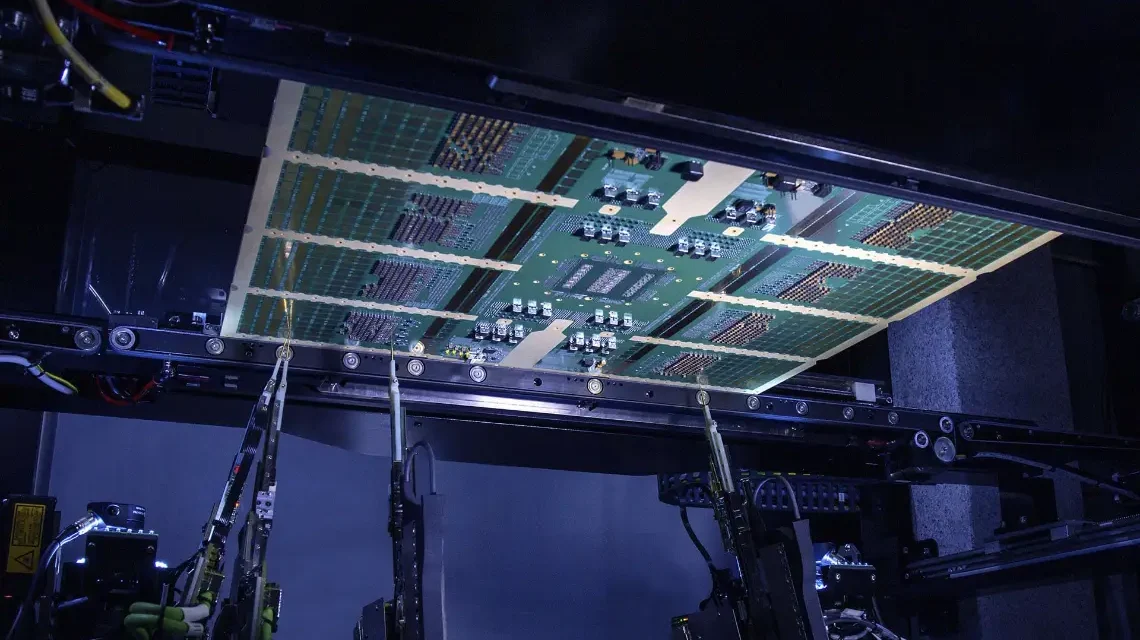
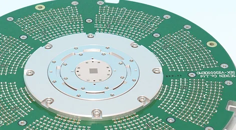
ATE Test PCB for Semiconductor and IC Testing An ATE Test PCB (Automated Test Equipment PCB) is a high-precision printed circuit board designed for semiconductor and integrated circuit testing systems. It serves as the electrical interface between the test system and the device under test (DUT), ensuring accurate signal transmission, stable power delivery, and reliable...

High Speed PCB – Precision Design for Signal Integrity and High Data Rate Applications

High Speed PCB for Modern Digital Systems As data rates continue to increase in communication, computing, and semiconductor applications, PCB design must evolve to maintain signal integrity and stable performance. A High Speed PCB is specifically engineered to support high-frequency digital signals, fast edge rates, and high bandwidth transmission. Unlike standard PCBs, high speed boards...

Microvia PCB – High Density Interconnect PCB for Advanced Electronic Applications

Microvia PCB for High Density Interconnect (HDI) Design As electronic products continue to shrink in size while increasing in functionality, traditional through-hole PCB structures are no longer sufficient. Microvia PCB technology enables higher routing density, improved signal integrity, and compact multilayer stackups, making it essential for modern high-performance electronics. Microvias are laser-drilled vias typically with...

IoT IC Test PCB – High Precision PCB for IoT Chip Testing Applications

What Is an IoT IC Test PCB? An IoT IC Test PCB is a specialized printed circuit board used for validating and testing integrated circuits (ICs) designed for Internet of Things (IoT) applications. These PCBs are commonly used in semiconductor test environments such as: Automated Test Equipment (ATE) systems Load boards Probe card assemblies Burn-in...

Load Board PCB – High Performance PCB for Semiconductor ATE Testing

What Is a Load Board PCB? A Load Board PCB is a critical component used in Automated Test Equipment (ATE) systems for semiconductor device testing. It provides the electrical interface between the ATE tester and the device under test (DUT), enabling accurate signal transmission, power delivery, and measurement. Load Board PCB is commonly used in:...

ATE Test PCB – High Precision PCB for Automated Test Equipment Applications

What Is an ATE Test PCB? An ATE Test PCB is a specialized printed circuit board designed for use in Automated Test Equipment (ATE) systems. It acts as the electrical interface between semiconductor devices and the test platform, enabling accurate signal transmission, power delivery, and measurement during IC testing. ATE Test PCB is commonly used...

Logic Test PCB – High Precision Test Boards for Digital and Logic IC Validation

What Is a Logic Test PCB? A Logic Test PCB is a specialized printed circuit board designed for testing and validating digital and logic integrated circuits (ICs). These boards are used in semiconductor development, production testing, and automated test equipment (ATE) systems to verify functionality, timing performance, and signal integrity of logic devices. Logic Test...

ATE PCB Supplier – High-Performance Test PCB Solutions for Semiconductor Testing

Who Is an ATE PCB Supplier? An ATE PCB Supplier is a professional manufacturer and solutions provider of printed circuit boards specifically designed for Automated Test Equipment (ATE) used in semiconductor testing. These suppliers deliver PCBs that serve as the electrical interface between ATE systems and devices under test (DUTs), enabling accurate functional, parametric, and...

Differential Pair PCB Design and Manufacturing for High-Speed Data Transmission

What Is a Differential Pair PCB? A Differential Pair PCB is a printed circuit board designed to route differential signal pairs, which are two complementary signals transmitted simultaneously to improve noise immunity, reduce crosstalk, and maintain signal integrity. Differential pair technology is critical in high-speed digital interfaces, such as USB, HDMI, PCIe, Ethernet, DDR memory,...

Fine Line PCB Manufacturing for High-Density and High-Performance Electronics

What Is a Fine Line PCB? A Fine Line PCB is a printed circuit board that uses extremely narrow traces and spaces to support high-density, complex electronic designs. Fine line technology is essential for applications where board real estate is limited but high-speed performance and signal integrity are required, such as smartphones, 5G modules, high-speed...