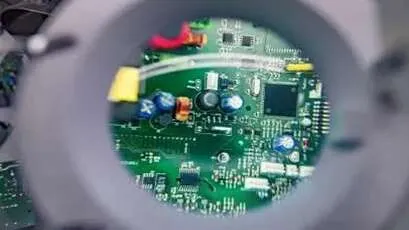
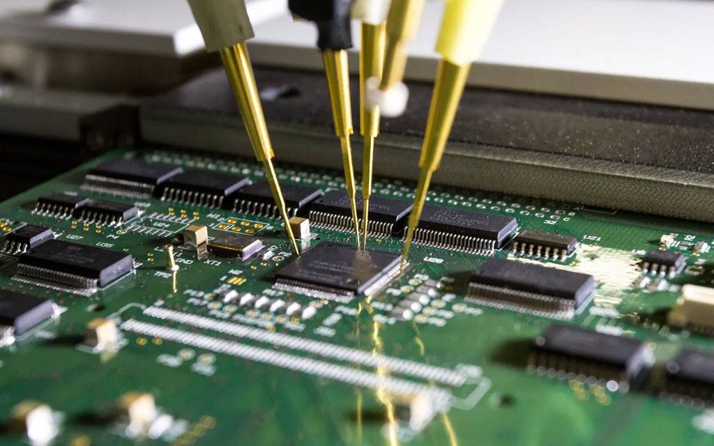
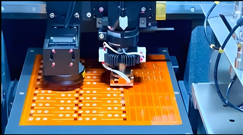
semiconductor test PCB - KKPCB
 
HomeTag

semiconductor test PCB - KKPCB

Probe Card PCB: Precision Interconnect Solutions for Wafer-Level Semiconductor Testing

Wafer-level testing is one of the most demanding stages in semiconductor manufacturing. At this level, accuracy, repeatability, and mechanical precision are critical. The Probe Card PCB serves as the core platform that connects automated test equipment (ATE) to semiconductor wafers, enabling precise electrical contact and reliable signal transmission during wafer probing. A high-quality Probe Card PCB...

ATE Test PCB: Ensuring Reliable and Repeatable Performance in Automated Test Systems

Automated Test Equipment (ATE) is the backbone of modern semiconductor validation and mass production. At the center of every ATE system is the ATE Test PCB, which directly affects test accuracy, yield stability, and long-term reliability. A well-engineered ATE test PCB ensures that measured performance reflects the device under test—not limitations of the test hardware....

Custom ATE PCB: Tailored Test Interfaces for Accurate and Scalable Semiconductor Testing

Automated Test Equipment (ATE) platforms are highly configurable, but their performance ultimately depends on how well the test interface matches the device under test. A Custom ATE PCB is specifically designed to bridge this gap by aligning electrical, mechanical, and system-level requirements for accurate and repeatable semiconductor testing. Unlike off-the-shelf boards, a custom ATE PCB...

Multilayer Test PCB: Building Stable and Scalable Platforms for Advanced Electronic Testing

As electronic devices and semiconductor systems grow more complex, test requirements evolve beyond what simple PCB structures can support. The Multilayer Test PCB provides the routing density, electrical isolation, and power stability required for accurate, repeatable testing across development and production stages. A professionally engineered Multilayer Test PCB ensures that test results remain consistent as...

HDI PCB: Advanced Interconnect Technology for Compact, High-Performance Electronics

As electronic devices become smaller, faster, and more complex, traditional PCB technologies often reach their physical limits. HDI PCB (High Density Interconnect PCB) technology was developed to overcome these challenges by enabling higher wiring density, finer geometries, and improved electrical performance. A professionally manufactured HDI PCB is a key enabler for modern consumer electronics, communication...

High Pin Count PCB: Enabling Dense Interconnection for Advanced Electronic and Semiconductor Systems

As electronic systems continue to integrate more functionality into smaller form factors, the number of signal, power, and ground connections continues to rise. The High Pin Count PCB is specifically engineered to manage thousands of interconnections while maintaining electrical integrity, mechanical reliability, and manufacturability. A professionally designed High Pin Count PCB is essential for modern...

Test Socket PCB: Ensuring Reliable Electrical Contact in High-Volume Semiconductor Testing

In semiconductor production testing, accurate results depend not only on test equipment and software but also on the physical interface between the device under test (DUT) and the test system. The Test Socket PCB plays a critical role by providing a stable electrical and mechanical foundation for test sockets used in engineering validation and mass...

Load Board PCB: Delivering Stable, High-Accuracy Interfaces for Semiconductor Production Testing

In high-volume semiconductor manufacturing, production testing must be fast, repeatable, and extremely reliable. At the center of this process is the Load Board PCB, a critical interface that connects automated test equipment (ATE) to the device under test (DUT). A well-designed Load Board PCB ensures that every device is evaluated under identical electrical conditions, enabling...

Semiconductor Test PCB: Ensuring Accuracy and Reliability Across the IC Testing Lifecycle

In semiconductor manufacturing, testing is not a single step—it is a continuous process that spans wafer probing, device validation, system-level testing, and mass production. At the core of this process lies the Semiconductor Test PCB, a specialized printed circuit board designed to deliver consistent electrical performance across every test stage. A well-designed Semiconductor Test PCB...

ATE Test PCB: Stabilizing Test Accuracy Across High-Speed and High-Volume IC Testing

In modern semiconductor production, test accuracy must remain stable not only for one device, but across tens of thousands—or even millions—of test cycles. While ATE systems continue to advance in speed and precision, the ATE test PCB remains a decisive factor in determining whether test results are repeatable, reliable, and production-ready. A professionally engineered ATE...