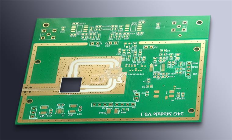
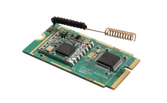
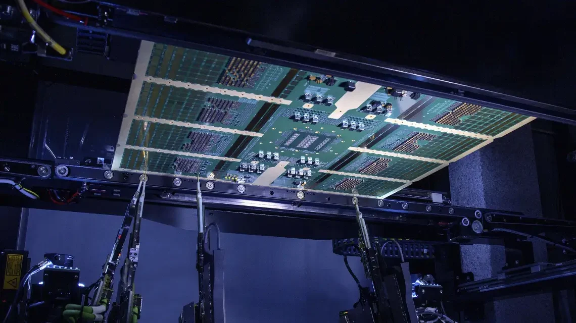
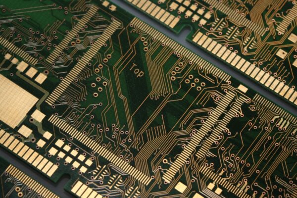
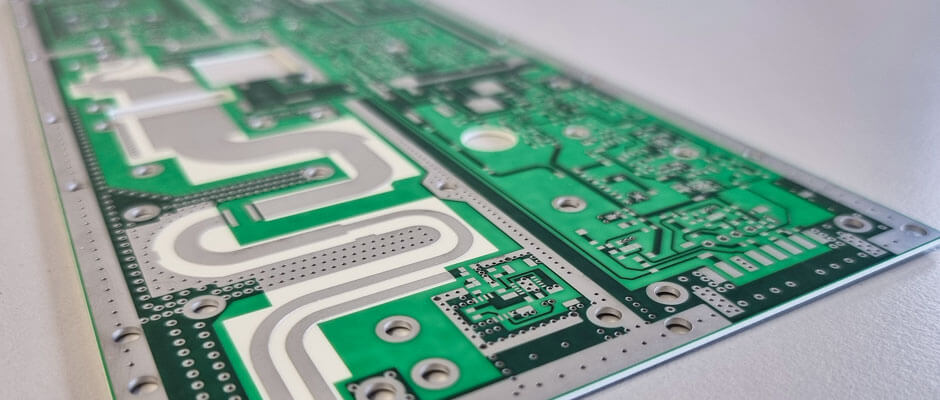
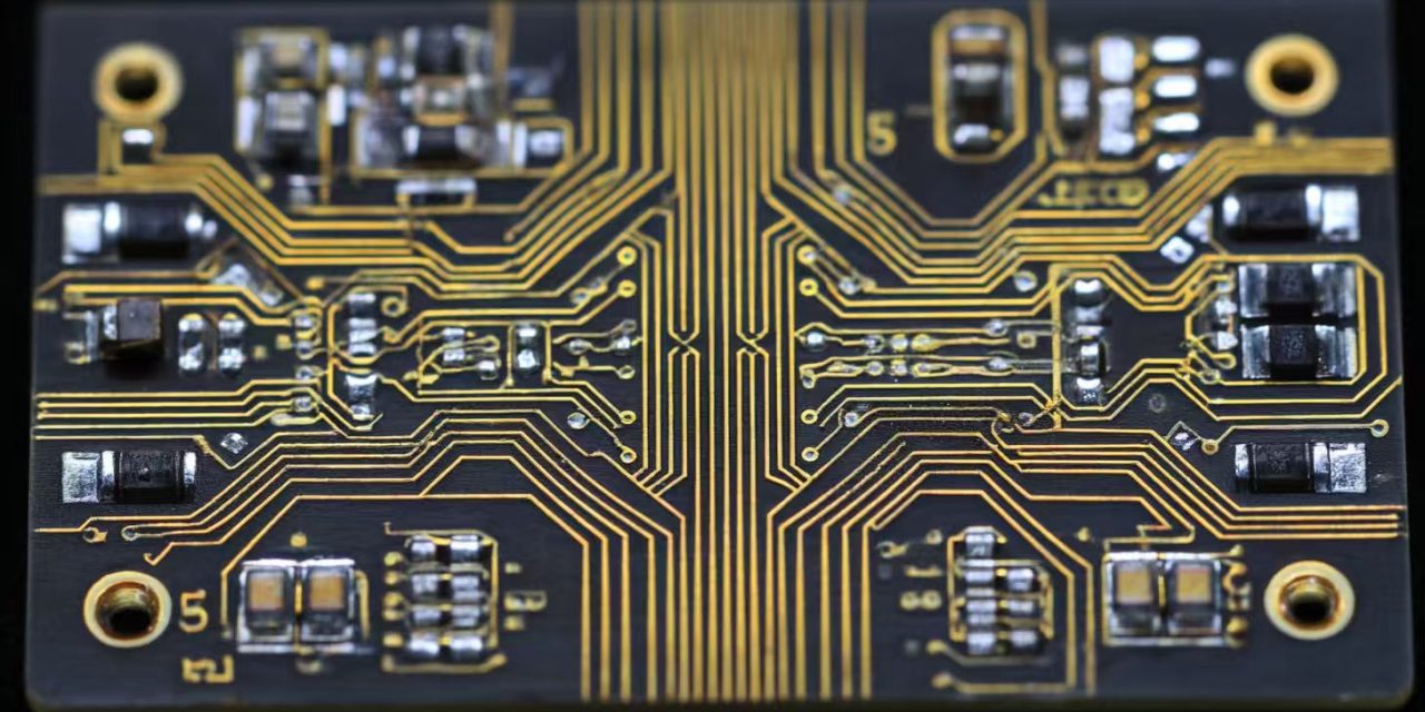
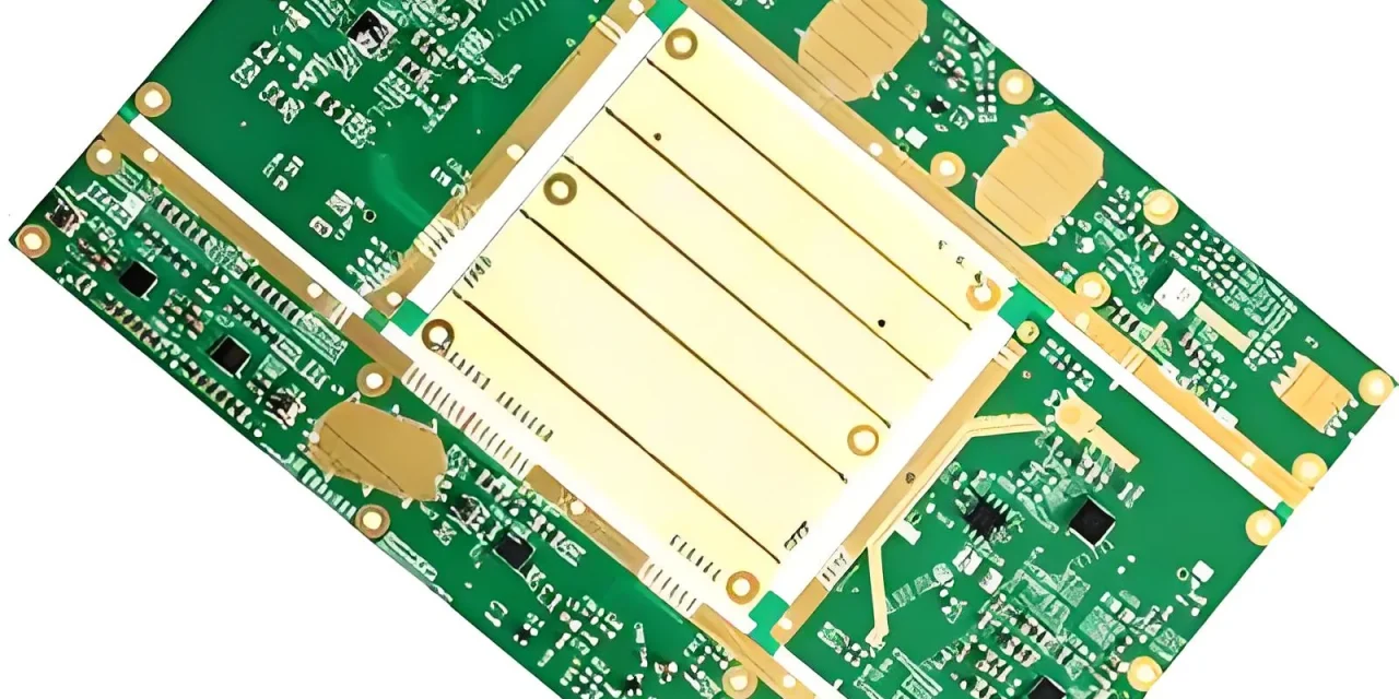
RF Test PCB - KKPCB
 
HomeTag

RF Test PCB - KKPCB

RF IC Test PCB: Precision PCBs for High-Frequency Semiconductor Testing

An RF IC Test PCB is a specialized semiconductor test circuit board designed to evaluate the electrical performance of radio frequency integrated circuits during wafer-level, package-level, or final testing stages. It is a critical interface within Automated Test Equipment (ATE) systems, enabling accurate measurement of RF parameters such as gain, noise figure, phase noise, insertion...

Automated Test Equipment PCB: High-Reliability PCBs for Precision Semiconductor Testing

An Automated Test Equipment PCB is a critical component used in ATE systems to perform functional, parametric, and reliability testing of semiconductor devices. These PCBs serve as the electrical interface between the test system and the device under test (DUT), ensuring accurate signal transmission, stable power delivery, and reliable measurement during high-volume semiconductor testing. As...

Automated Test Equipment PCB: Reliable PCB Solutions for Advanced Semiconductor Testing

As semiconductor devices move toward higher speed, higher pin count, and higher integration, testing accuracy has become a key factor in product quality and yield. Automated Test Equipment (ATE) PCBs are at the heart of modern semiconductor testing systems, providing a stable and high-performance interface between devices under test (DUTs) and automated test platforms. A...

RF IC Test PCB: High-Frequency Test Solutions for RF and Wireless Semiconductor Devices

With the rapid advancement of 5G, IoT, Wi-Fi, and mmWave technologies, RF integrated circuits (RF ICs) are becoming increasingly complex and high-speed. Ensuring accurate characterization and validation of these devices requires specialized RF IC Test PCBs capable of maintaining signal integrity at high frequencies. A well-designed RF IC Test PCB serves as the critical interface...

High Frequency Test PCB: Ensuring Measurement Accuracy in RF and Microwave Validation

In RF, microwave, and high-speed electronic testing, even minor PCB imperfections can introduce significant measurement errors. The High Frequency Test PCB is engineered to serve as a neutral and stable signal platform, allowing engineers to evaluate devices and systems with confidence. A properly designed high frequency test PCB ensures that test results reflect device performance—not...

High Frequency Test PCB: Precision Design and Low-Loss Materials for Accurate RF and High-Speed Testing

As RF, microwave, and high-speed digital technologies continue to advance, test environments must deliver exceptional signal fidelity. The High Frequency Test PCB is specifically designed to support precise signal transmission, minimal loss, and repeatable measurement results at high frequencies. A properly engineered high frequency test PCB is essential for reliable RF and high-speed validation. What...

High Frequency Test PCB: Achieving Accurate and Repeatable Measurements at RF and Microwave Frequencies

Testing high-frequency circuits is fundamentally different from testing standard digital electronics. At RF and microwave frequencies, even small PCB variations can introduce loss, phase error, or impedance mismatch that directly distort test results. The High Frequency Test PCB is specifically engineered to provide a stable and predictable platform for accurate RF measurement and validation. A...

RF Test PCB: Engineering Precision for High-Frequency Testing Systems

RF Test PCB: Engineering Precision for High-Frequency Testing Applications Introduction As wireless communication, semiconductor devices, and high-frequency electronics continue to advance, the demand for precise and reliable test platforms has increased dramatically. Among these platforms, the RF Test PCB plays a central role. It enables engineers to validate RF performance, measure high-frequency characteristics, and ensure...