
The Importance of High Frequency Test PCB in RF Validation
Testing high-frequency circuits requires significantly higher precision than conventional digital electronics testing. At RF and microwave frequencies, even minor variations in PCB materials, geometry, or manufacturing processes can introduce signal loss, phase deviation, impedance mismatch, and measurement errors.
A High Frequency Test PCB is specifically designed to provide a stable and predictable testing platform for RF, microwave, and high-speed analog circuit validation. It ensures that measured results accurately represent the actual performance of the device under test (DUT), rather than being influenced by limitations of the test board itself.
Unlike standard application PCBs, high-frequency test boards prioritize:
- Electrical accuracy
- Low signal loss
- Controlled impedance
- Signal repeatability
- Mechanical stability during testing
What Is a High Frequency Test PCB?
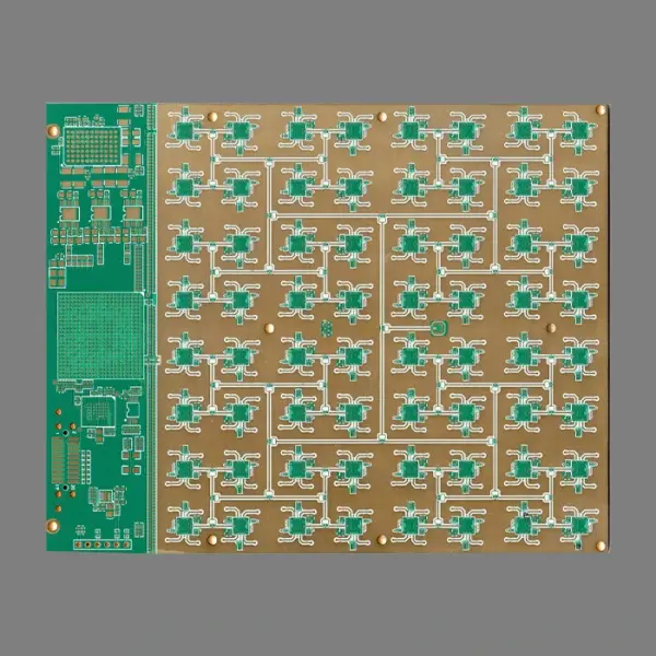
A High Frequency Test PCB is a specialized printed circuit board used for evaluating RF, microwave, and high-speed analog devices. It functions as the electrical interface between:
- RF test instruments and ATE systems
- Devices under test (DUTs)
- RF connectors, probes, and test sockets
These PCBs are engineered to maintain consistent electrical characteristics under demanding test conditions, enabling accurate characterization and validation of high-frequency devices.
Why High Frequency Test PCB Quality Matters
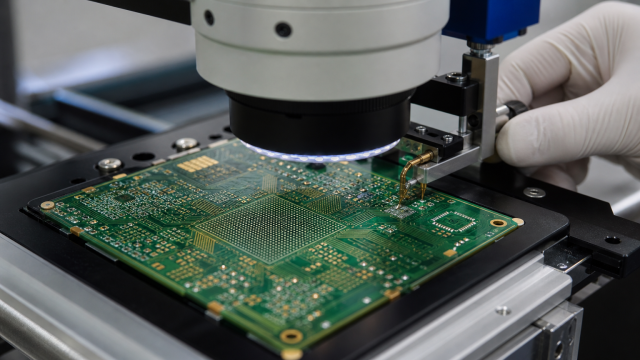
At high frequencies, PCB performance directly affects measurement accuracy. Poor PCB design or manufacturing control may introduce:
- Excessive insertion loss
- Impedance mismatch and signal reflection
- Phase instability
- Timing deviation
- Increased measurement uncertainty
A reliable High Frequency Test PCB minimizes these effects by maintaining stable transmission characteristics and ensuring repeatable RF measurements.
Key Design Considerations for High Frequency Test PCBs
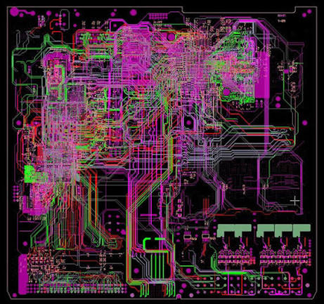
1. Controlled Impedance and Transmission Line Accuracy
Precise impedance control is one of the most important requirements for high-frequency test boards.
Variations in impedance can lead to:
- Signal reflection
- Reduced power transfer efficiency
- Measurement distortion
Effective impedance control requires:
- Accurate trace width and spacing design
- Consistent dielectric thickness
- Stable reference plane structures
- Proper transmission line modeling
- Manufacturing impedance verification
Maintaining impedance consistency ensures reliable RF signal propagation throughout the test path.
2. Low-Loss Materials and Signal Transmission Performance
As operating frequencies increase, dielectric loss and conductor loss become major factors affecting signal quality.
High Frequency Test PCBs typically utilize:
- Low-Dk and low-Df RF laminates
- Rogers and PTFE-based materials
- Hybrid RF and FR-4 stack-up solutions
- Low-roughness copper for improved high-frequency performance
Optimized material selection helps reduce insertion loss and preserve signal integrity during RF measurements.
3. Signal Integrity and Crosstalk Control
High-frequency signals are highly sensitive to unwanted coupling and electromagnetic interference.
Common design challenges include:
- Crosstalk between adjacent RF traces
- Uncontrolled return current paths
- Electromagnetic interference (EMI)
Effective solutions include:
- Optimized RF trace spacing
- Dedicated reference planes
- Ground isolation structures
- Proper layer assignment
- Shielding via structures
These techniques help maintain signal purity and measurement accuracy.
4. RF Connector and Interface Transition Design
The transition between connectors and PCB transmission lines is a critical area in high-frequency testing.
Poor interface design may cause:
- Impedance discontinuity
- Additional reflection
- Phase error
Reliable designs require:
- Smooth impedance transitions
- Proper grounding around RF connectors
- Optimized connector launch structures
- Mechanical reinforcement for repeated connections
Well-designed interfaces improve measurement consistency and reduce test variation.
5. Stack-Up Design and Material Stability
PCB stack-up directly influences electrical performance and mechanical reliability.
Important considerations include:
- Symmetrical multilayer structures
- Controlled dielectric thickness
- Stable RF laminate properties
- Hybrid material compatibility
A properly engineered stack-up provides consistent impedance performance and minimizes variation during manufacturing.
Mechanical Reliability and Test Repeatability
High Frequency Test PCBs often experience repeated connections, thermal changes, and mechanical stress during operation.
Long-term reliability depends on:
- Excellent PCB flatness
- Controlled warpage
- Balanced layer construction
- Reinforced connector mounting areas
Mechanical stability is essential because physical variation can directly affect electrical performance and test repeatability.
Manufacturing Precision and RF Verification
For high-frequency applications, manufacturing consistency is as important as PCB design.
Key manufacturing requirements include:
- Tight laminate thickness control
- Precise drilling and etching
- Accurate layer registration
- Controlled impedance fabrication
- RF performance verification
Strict process control ensures consistent electrical characteristics from prototype development to production quantities.
Applications of High Frequency Test PCBs
High Frequency Test PCBs are widely used in:
- RF and microwave circuit validation
- 5G and mmWave module testing
- Antenna and RF front-end evaluation
- High-speed analog circuit testing
- Wireless communication device validation
- Semiconductor RF characterization
These applications require highly accurate, low-loss, and repeatable testing environments.
Selecting the Right High Frequency Test PCB Manufacturer
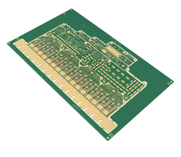
Choosing an experienced manufacturing partner is essential for achieving reliable RF test performance.
Important capabilities include:
- Experience with RF and microwave PCB fabrication
- Low-loss material processing capability
- Controlled impedance manufacturing
- RF testing and verification support
- Engineering collaboration during design optimization
A capable partner helps reduce measurement uncertainty, accelerate validation cycles, and improve product development efficiency.
Conclusion: Enabling Accurate RF and Microwave Testing
A High Frequency Test PCB is a critical foundation for accurate RF and microwave measurement. Through precise impedance control, low-loss material selection, optimized signal integrity design, and advanced manufacturing processes, high-frequency test boards enable reliable and repeatable device validation.
As wireless technologies continue advancing toward higher frequencies and greater bandwidth, selecting a qualified High Frequency Test PCB manufacturer becomes increasingly important for achieving consistent test performance and faster product development.
