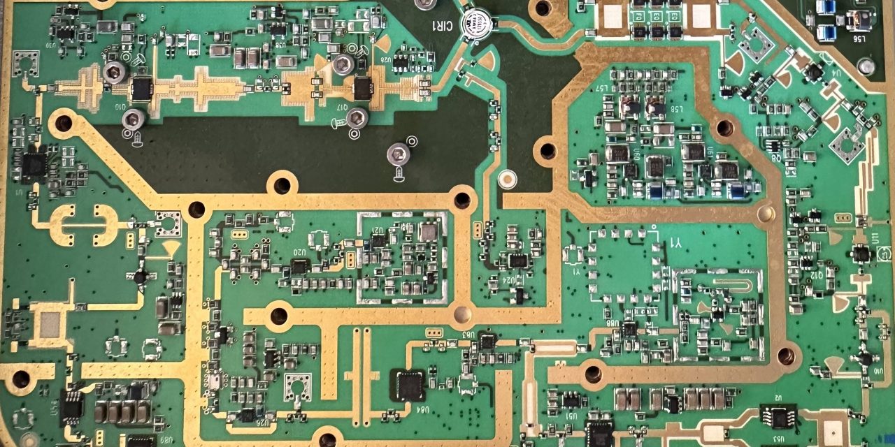
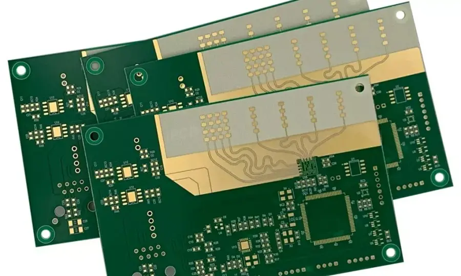
RF Signal Integrity - KKPCB
 
HomeTag

RF Signal Integrity - KKPCB

Enhance Multi-Layer Impedance Control and Low-Loss Performance Using TLY-5 PCB for mmWave Communication Systems

1. Engineering Context Next-generation mmWave communication systems—including 5G base stations, satellite payloads, and radar modules—require PCBs that provide ultra-stable impedance, low insertion loss, and phase-consistent routing. Traditional FR-4 or high-speed laminates often suffer from dielectric drift, higher Df, and thermal expansion issues, which degrade signal fidelity, EMI immunity, and system reliability in dense multi-layer RF...

Optimize Low-Loss Signal Chains and EMI Control Using RF Transceiver PCB Designs for High-Frequency Communication Systems

High-frequency communication systems—from 5G NR radios and phased-array front ends to satellite downlink modules and wideband radar—rely on precisely engineered RF Transceiver PCB architectures to maintain low-loss signal chains, stable phase performance, and strong EMI suppression. As operating frequencies rise into sub-6 GHz, C-band, Ku-band, Ka-band and even mmWave ranges, the electrical behavior of the...

Design Next-Gen Satellite Communication Systems with RO4835 PCB for Precise Impedance Control and Wideband Consistency

Satellite communication systems require ultra-stable RF performance across wide frequency bands, often spanning Ka- and Ku-bands. Maintaining precise impedance control, minimal insertion loss, and consistent phase response is critical for antenna feeds, transceivers, and payload modules. RO4835 PCB laminates (Dk = 3.48 ± 0.03, Df = 0.0037 @10 GHz) offer low-loss, thermally stable dielectric properties,...

Optimize Thermal Performance and EMI Suppression in High-Density RF Modules with Low Loss PCB Materials

High-density RF modules used in 5G radios, SATCOM terminals, phased-array beamformers, and mmWave front-end units are increasingly constrained by thermal stress, EMI coupling, and insertion loss. As operating frequencies push beyond 10–40 GHz, traditional FR-4 structures can no longer maintain stable impedance, consistent dielectric behavior, or low-loss routing. This is where Low Loss PCB materials—such...

Enhance Signal Integrity and Thermal Reliability in Multilayer Blind Via PCBs for High-Density RF Modules

High-density RF modules in 5G base stations, satellite payloads, and advanced IoT systems require compact multilayer PCBs with precise signal routing, minimal crosstalk, and high thermal resilience. Blind via technology allows for efficient vertical interconnects while reducing PCB stackup thickness, improving high-frequency performance, and maintaining signal integrity across densely packed layers. KKPCB integrates precision lamination,...

Enhance Power Density and EMI Immunity Using Multilayer UAV PCB Stackups for Autonomous Flight Control Systems

Autonomous UAV flight control systems demand high power density PCB designs capable of handling dense interconnects, high-frequency control signals, and EMI-sensitive power circuits. Compact UAV architectures leave minimal space for routing, making multilayer PCB stackups essential for maintaining signal fidelity, phase stability, and electromagnetic compatibility. Multilayer UAV PCBs enable segregated power and control planes, optimized...

Optimize Phase-Stable High-Frequency Routing with Blind Via PCB Architectures in Compact Satellite Communication Payloads

Compact satellite communication payloads require precise, phase-stable RF routing to maintain signal fidelity and low insertion loss across high-frequency channels. The limited space and high-density requirements make blind via architectures essential for multilayer PCBs, enabling signal interconnects without penetrating all layers, reducing parasitic capacitance, and controlling crosstalk. Blind via PCBs allow compact routing of RF...

Minimize Crosstalk and Maintain Impedance Precision Using Advanced Blind Via PCB Layouts in 5G mmWave Systems

5G mmWave hardware doesn’t leave much room for layout mistakes. When operating above 24 GHz, a few microns of misalignment, a poorly shaped via stub, or an uncontrolled dielectric transition can collapse RF integrity. That is why advanced blind via PCB layouts have become a core enabling technology for minimizing crosstalk, stabilizing impedance, and preserving...

Optimize RF Signal Integrity and Lightweight HDI UAV PCB Architectures for Next-Gen Drone Navigation Modules

Next-generation UAV systems—whether used for industrial IoT sensing, long-range inspection, autonomous mapping, or precision agriculture—depend on PCB platforms capable of delivering high-frequency RF accuracy, ultra-stable GNSS/GPS reception, multi-band communication reliability, and lightweight HDI construction. As flight durations extend and sensor payloads grow more complex, the PCB becomes the backbone that determines navigation precision, RF sensitivity,...

Optimize High-Frequency UAV PCB Architectures to Enhance IoT Crop Monitoring, Precision Spraying, and Long-Range Agricultural Drone Communication

IoT-enabled agricultural UAVs operate in a uniquely demanding environment: wide temperature swings, continuous vibration, variable humidity, and rapidly changing RF propagation conditions over open farmland. These drones must maintain long-range wireless links, collect high-resolution crop data, and execute precision-controlled spraying while keeping power consumption and mass as low as possible. To meet these requirements, modern...