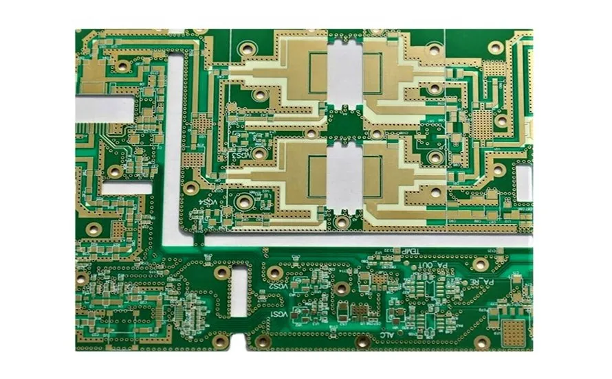
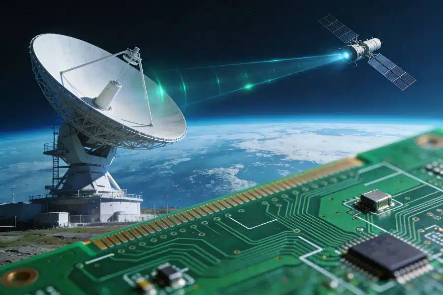
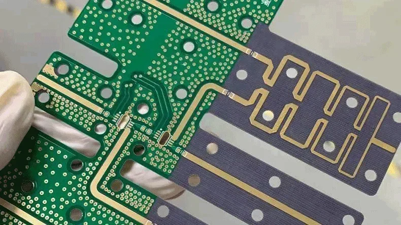
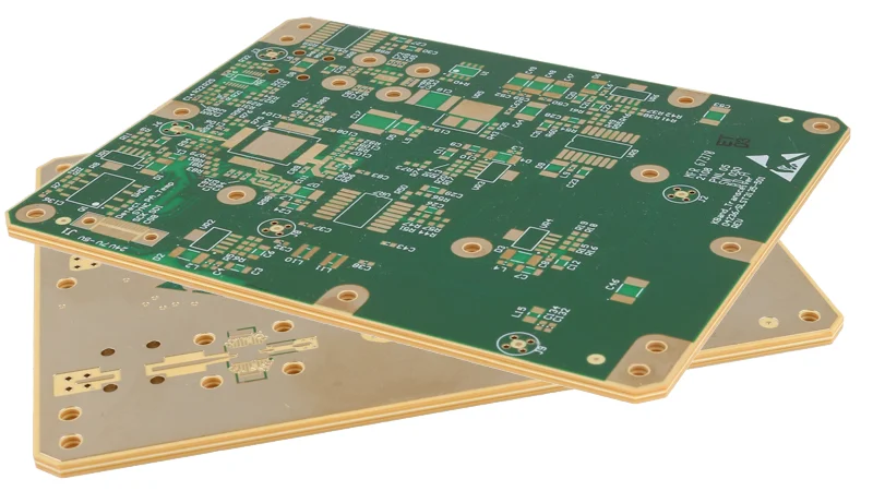
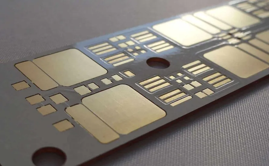
RF PCB - KKPCB
 
HomeTag

RF PCB - KKPCB

Optimizing High-Frequency Stability and Low-Loss Transmission Using RF-35 PCB Laminates for Modern Wireless Systems

RF-35 PCB laminates operate in a class where dielectric precision directly shapes RF linearity, bandwidth uniformity, and system-level efficiency. Modern wireless products—Wi-Fi 6/7 modules, IoT gateways, sub-6 GHz links, and microwave-band transceivers—depend on stable Dk/Df behavior to maintain predictable impedance and low insertion loss. RF-35 offers a low-loss dielectric platform designed for controlled RF propagation,...

High-Frequency Signal Integrity Optimization and Phase-Stable Transmission with Megtron 7 PCB Substrates in 5G Server and High-Speed Computing Systems

Megtron 7 PCB laminates are widely adopted in 5G servers, AI computing accelerators, and cloud networking equipment due to their exceptionally low dielectric loss and superior stability at 28–112 Gbps PAM4 and mmWave bands. As system architectures transition toward high-density multi-lane SerDes and advanced RF interconnects, PCB materials become a primary constraint influencing channel loss...

High-frequency Wi-Fi 6/7 antenna modules in modern laptops demand PCBs that maintain low insertion loss, precise phase alignment, and robust EMI suppression within compact layouts. TLY-5 PCB laminates, with a dielectric constant of 3.45 ± 0.03 and dissipation factor of 0.0012 @10 GHz, provide low-loss RF transmission and dimensional stability essential for multi-band performance. KKPCB...

Low-Loss Transmission and EMI Control of Ceramic PCBs in Satellite Communication and High-Frequency Payload Units

Engineering Context / Abstract   In modern satellite communication systems, RF payload units demand precise signal transmission, minimal insertion loss, and robust EMI suppression. High-frequency payloads, including Ku- and Ka-band transceivers, operate under extreme thermal, vacuum, and radiation conditions, where even minor dielectric fluctuations can cause phase errors and signal degradation.   Ceramic PCB substrates,...

High-Density Power Integrity and Heat Dissipation Optimization Using Ceramic PCB Substrates in Laptop Motherboards and Wi-Fi 7 Systems

Engineering Context / Abstract   Modern laptop motherboards and Wi-Fi 7 modules demand exceptional power integrity and efficient thermal management due to the increasing density of integrated circuits, high-speed memory buses, and advanced RF front-end modules. Ceramic PCB substrates, featuring low dielectric loss (Df = 0.0015 @10GHz) and stable dielectric constant (Dk = 9.8 ±...

Low Loss PCBs Explained: Materials, Features & High-Frequency Performance

What Is a Low Loss PCB? Premium Materials, Performance Advantages & Applications In high-frequency electronics, signal integrity is everything. As data rates climb and RF systems move into the mmWave range, traditional FR-4 PCBs quickly become inadequate due to excessive dielectric loss, copper loss and thermal instability. At KKPCB, we engineer Low Loss PCBs specifically...

RF Amplifiers Explained: Essential Knowledge for PCB Electronics Manufacturers

Essential RF Amplifier Knowledge for Modern PCB Manufacturers | KKPCB As wireless communication, IoT connectivity, radar sensing, and high-speed data links continue to evolve, RF amplifiers have become one of the most critical building blocks in modern electronics. For PCB manufacturers, understanding how RF amplifiers work—and how PCB design impacts their performance—is essential to delivering...

Radar PCB Design: Materials, High-Frequency Layout Techniques & Applications

Radar PCB: Design Principles, Materials, Manufacturing Challenges & Key Applications High-speed PCBs stand at the top of modern circuit-board technology, spanning digital high-speed, mixed-signal, and RF/microwave categories. Among these, RF and microwave PCBs operate at the highest frequencies, making them essential for advanced applications—especially RADAR (Radio Detection and Ranging). Because Radar PCBs frequently host a...

RF PCB Design for 5G Devices: Antenna Integration, Impedance Control & High-Frequency Layout Guide

RF PCB Design for 5G Devices: High-Frequency Architecture, Antenna Integration & Engineering Best Practices Designing RF PCBs for 5G hardware is far more than simple high-speed layout—it requires a deep command of electromagnetic behavior, antenna engineering, high-frequency signal routing, impedance control, and noise isolation.In next-generation wireless systems, the antenna is no longer a passive component—it...

Taconic TLY-5 PCB Material: A Complete Technical Guide for High-Frequency, RF, and Microwave Applications

Taconic TLY-5 PCB Laminates: Ultra-Low-Loss Materials for High-Frequency Excellence In high-frequency PCB engineering, materials are the foundation of performance. From RF front-ends to satellite communication systems, every decibel of loss, every fluctuation in dielectric stability, and every thermal deviation directly impacts system integrity. Taconic TLY-5 stands out as one of the industry’s most trusted PTFE-based...