
Engineering Context
As operating frequencies continue to increase across 5G communication, Wi-Fi 7, automotive radar, satellite communication, and microwave RF systems, traditional FR-4 materials can no longer meet the stringent electrical requirements of high-frequency circuit design. Increased dielectric loss, unstable impedance, and inconsistent phase characteristics can significantly degrade system performance.
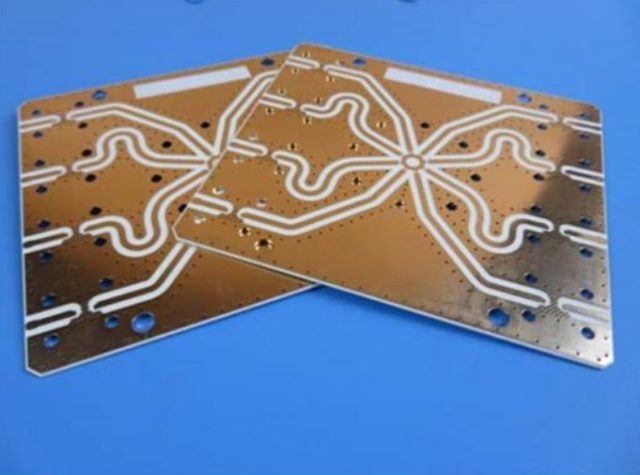
Rogers PCB technology has become one of the industry’s preferred solutions for high-frequency applications due to its stable dielectric constant (Dk), low dissipation factor (Df), excellent thermal performance, and outstanding dimensional stability. Rogers laminates—including RO4350B PCB, RO3003 PCB, RO4835 PCB, and RO5880 PCB—enable engineers to achieve predictable RF performance while reducing insertion loss and maintaining signal integrity across wide frequency ranges.
Unlike conventional PCB materials, Rogers laminates are specifically engineered for RF and microwave circuits where impedance control, phase consistency, and low-loss transmission directly influence communication quality, antenna efficiency, and radar accuracy.
For both RF engineers and purchasing professionals, selecting the appropriate Rogers material involves balancing electrical performance, manufacturability, thermal reliability, lead time, and total project cost.
KKCPB specializes in the fabrication of Rogers PCBs, hybrid multilayer RF boards, and controlled impedance solutions for telecommunications, aerospace, defense, automotive electronics, and industrial wireless systems.
Core Engineering Challenges
Designing and manufacturing high-frequency Rogers PCBs involves much more than selecting a premium laminate. Every stage—from stackup planning to lamination and impedance verification—affects final RF performance.
| Engineering Challenge | Root Cause | Engineering Impact |
|---|---|---|
| High insertion loss | Inappropriate dielectric material or copper roughness | Reduced RF transmission efficiency |
| Impedance variation | Stackup tolerance and etching deviation | Signal reflection and degraded SI |
| Phase inconsistency | Dk variation and dielectric thickness changes | Beamforming and timing errors |
| Hybrid lamination difficulty | Different CTE between Rogers and FR-4 | Delamination and registration issues |
| EMI coupling | Dense RF routing | Crosstalk and receiver sensitivity reduction |
| Thermal deformation | Continuous high-power RF operation | Reliability reduction |
These challenges are particularly critical in RF PCB, Microwave PCB, 5G Antenna PCB, Automotive Radar PCB, and Satellite Communication PCB applications where stable electromagnetic performance determines overall system reliability.
Material Science & Dielectric Performance
Rogers offers multiple laminate families optimized for different RF frequencies, thermal environments, and manufacturing requirements.
Comparison of Common Rogers PCB Materials
| Material | Typical Dk | Typical Df (@10 GHz) | Typical Applications | Engineering Advantages |
|---|---|---|---|---|
| RO3003 PCB | 3.00 ±0.04 | 0.0013 | Phase-critical microwave circuits | Excellent phase stability |
| RO4350B PCB | 3.48 ±0.05 | 0.0037 | 5G, RF amplifiers, wireless infrastructure | Cost-effective RF performance |
| RO4835 PCB | 3.48 | 0.0031 | High-power RF systems | Improved oxidation resistance |
| RO5880 PCB | 2.20 ±0.02 | 0.0009 | mmWave, satellite, aerospace | Ultra-low dielectric loss |
Key Electrical Properties
| Parameter | Typical Value | Engineering Benefit |
|---|---|---|
| Stable Dielectric Constant (Dk) | Tight tolerance | Accurate impedance control |
| Low Dissipation Factor (Df) | 0.0009–0.0037 | Reduced insertion loss |
| Low Moisture Absorption | <0.1% | Stable RF performance in harsh environments |
| Excellent Thermal Stability | High Tg and low CTE | Reliable multilayer lamination |
| Dimensional Stability | Excellent | Improved registration accuracy |
Compared with conventional FR-4 materials, Rogers laminates significantly reduce signal attenuation and improve phase consistency, making them ideal for multilayer RF and microwave PCB designs.
KKCPB Case Study — RO4350B PCB for 5G RF Front-End Module
Client & Application Context
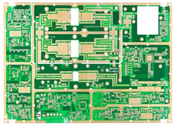
A global telecommunications equipment manufacturer approached KKCPB to develop an 8-layer RO4350B PCB for a compact 5G RF front-end module deployed in outdoor small-cell base stations.
The PCB integrated:
- Power amplifiers (PAs)
- Low-noise amplifiers (LNAs)
- RF filters
- Beamforming control circuits
- High-speed digital interfaces
- 5G antenna feed networks
The customer required low insertion loss, excellent impedance consistency, and scalable manufacturing for high-volume deployment.
Engineering Problem
The customer’s previous multilayer RF PCB exhibited several issues:
- Insertion loss exceeded design targets above 6 GHz
- Impedance variation reached ±6%
- RF channel phase mismatch affected beamforming performance
- Delamination occurred after repeated lead-free reflow cycles
- EMI coupling between RF and digital sections reduced receiver sensitivity
These problems increased tuning time during module assembly and negatively impacted production yield.
KKCPB Engineering Solution
KKCPB redesigned the RF PCB using a hybrid architecture centered on RO4350B PCB material.
The solution included:
- RO4350B laminates for RF signal layers
- High-Tg FR-4 for digital control and power routing
- Optimized hybrid stackup for thermal balance
- Controlled impedance routing with ±2% tolerance
- Low-profile copper foil to reduce conductor loss
- Ground plane segmentation for EMI isolation
- Via back-drilling to minimize signal reflections
- Dedicated RF impedance coupons for production verification
Complete design validation was performed before fabrication using HFSS, ADS, TDR, and Thermal FEM simulations.
Measured Results
| Parameter | Design Target | KKCPB Result |
|---|---|---|
| Controlled Impedance | ±5% | ±1.5% |
| Insertion Loss @6 GHz | <0.30 dB/in | 0.22 dB/in |
| Return Loss (S11) | < –15 dB | –19.4 dB |
| Phase Deviation | <1° | 0.38° |
| EMI Coupling | Minimized | Reduced by 37% |
| Layer Registration | ±25 μm | ±12 μm |
| Production Yield | >95% | 99.0% |
Project Outcome
The optimized RO4350B PCB significantly improved RF signal integrity while reducing manufacturing variation across production lots.
The customer achieved:
- Improved beamforming accuracy
- Lower RF insertion loss
- Higher receiver sensitivity
- Reduced RF calibration time
- Increased manufacturing yield
- Lower overall production costs
The project successfully transitioned from engineering validation into high-volume manufacturing with consistent electrical performance.
Stackup Design & RF Implementation
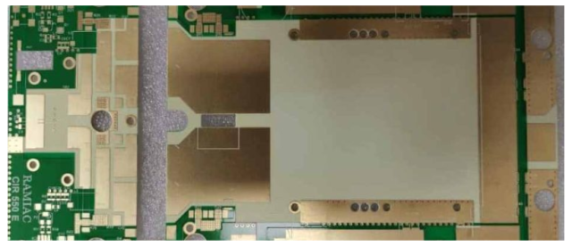
Representative 8-LLayer Rogers Hybrid PCB Stackup
| Layer | Function | Material |
|---|---|---|
| L1 | RF Signal Layer | RO4350B PCB |
| L2 | Ground Plane | Copper |
| L3 | RF Routing | RO4350B PCB |
| L4 | Power Plane | High-Tg FR-4 |
| L5 | Digital Signals | High-Tg FR-4 |
| L6 | Ground Plane | Copper |
| L7 | RF Interface Layer | RO4350B PCB |
| L8 | Bottom Control Layer | High-Tg FR-4 |
Simulation & Validation
KKCPB combines advanced simulation with comprehensive production verification to ensure predictable RF performance.
HFSS Simulation
- Electromagnetic field analysis
- Antenna feed optimization
- Coupling and radiation evaluation
- RF transition optimization
ADS Circuit Simulation
- S-parameter optimization
- Gain and insertion loss prediction
- Phase matching verification
- RF network analysis
TDR Measurement
- Controlled impedance verification
- Differential pair analysis
- Via transition validation
Thermal FEM Simulation
- Power amplifier thermal modeling
- Heat dissipation optimization
- Thermal expansion prediction
Manufactured boards are further verified through AOI inspection, X-ray analysis, impedance coupon testing, and Vector Network Analyzer (VNA) measurements to ensure excellent correlation between simulation and production.
Environmental & Reliability Validation
| Test | Condition | KKCPB Result |
|---|---|---|
| Thermal Cycling | −40°C ↔ +125°C, 1000 cycles | No delamination |
| High Temperature Storage | 150°C, 1000 h | Stable dielectric properties |
| Humidity Test | 85°C / 85% RH, 1000 h | Dk shift <0.02 |
| Lead-Free Solder Reflow | 260°C ×3 cycles | No warpage |
| Mechanical Vibration | 5–500 Hz, 10G | No via cracking |
| RF Stability Test | Continuous high-power operation | Stable insertion loss and phase consistency |
These tests demonstrate the long-term reliability of Rogers PCBs in demanding RF and microwave operating environments.
Engineering Summary & Contact
Rogers PCB technology has become the benchmark for high-frequency electronic systems requiring low insertion loss, stable impedance, and exceptional phase consistency. Whether designing a 5G RF Front-End Module, Microwave Communication System, Automotive Radar PCB, Satellite Payload, or Industrial Wireless Platform, Rogers laminates provide the electrical performance necessary for next-generation RF applications.
For engineers, selecting the right Rogers material—such as RO3003 PCB for phase-critical circuits, RO4350B PCB for balanced RF performance, RO4835 PCB for enhanced oxidation resistance, or RO5880 PCB for ultra-low-loss microwave designs—is essential to achieving both technical and commercial success.
KKCPB provides end-to-end Rogers PCB manufacturing services, including material selection, stackup optimization, RF simulation, controlled impedance fabrication, prototype development, and high-volume production. Our engineering team works closely with OEMs, RF designers, and procurement professionals to deliver reliable, cost-effective PCB solutions for advanced RF, microwave, and 5G communication systems.
