RF Communication PCB - KKPCB
 
HomeTag

RF Communication PCB - KKPCB

RF Trace PCB: Precision RF Routing for High-Frequency and Low-Loss Signal Transmission

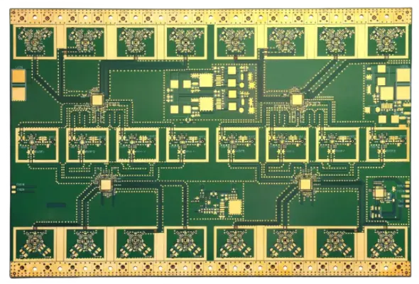
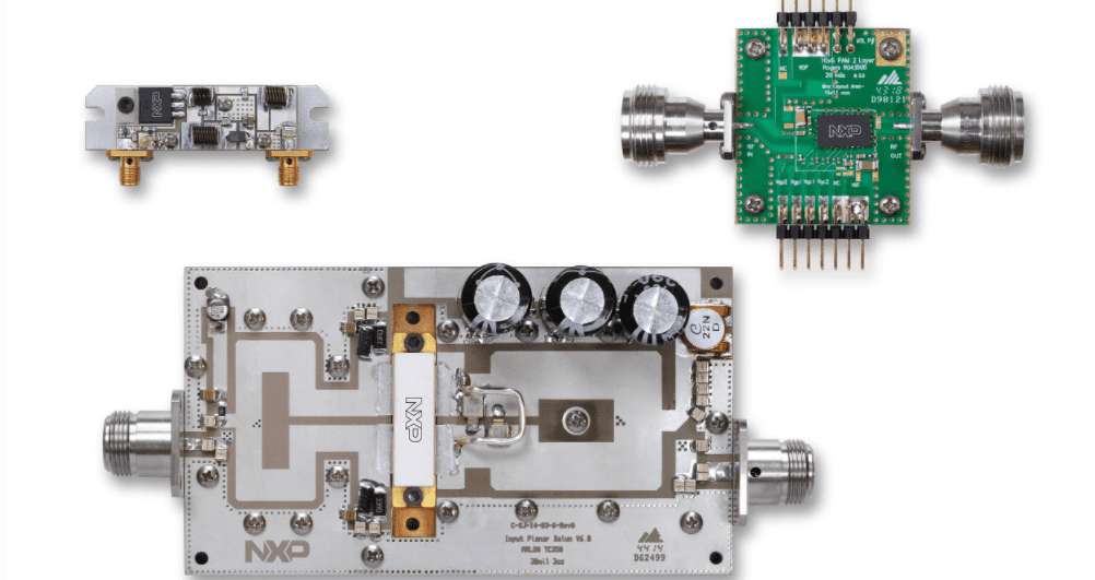
An RF Trace PCB is a specialized printed circuit board designed for RF signal transmission and high-frequency applications, where signal loss, impedance stability, and EMI control are critical. As wireless technologies such as 5G, WiFi, GPS, IoT, and radar systems continue to grow, RF PCB performance requirements become stricter than ever. Unlike ordinary digital traces,...

Achieve Low-Loss Transmission and Stable Impedance Performance with Double Layer HF PCB Engineering for High-Frequency Communication Systems

A Double Layer HF PCB may appear structurally simple, yet in high-frequency engineering it provides a remarkably efficient platform for low-loss propagation, stable impedance, and predictable electromagnetic behavior. When RF designers need high-frequency stability without the cost or stackup escalation of multilayer PCBs, a Double Layer HF PCB offers the ideal balance between manufacturability and...

Drive Ultra-Stable Dk/Df Performance and High-Power Efficiency Using RO5880 PCB Architectures in Mission-Critical Aerospace and Communication Systems

Mission-critical aerospace and high-frequency communication systems depend on PCB materials that deliver absolute electrical stability, consistent power efficiency and repeatable RF performance under extreme thermal, mechanical and radiation environments. RO5880 PCB architectures have become a foundation for these systems because they offer exceptionally stable Dk/Df, low insertion loss and predictable phase behavior across microwave and...