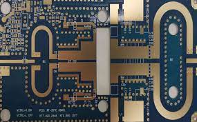
mmWave PCB design - KKPCB
 
HomeTag

mmWave PCB design - KKPCB

Low-Loss RF Filter and Coupler Design Using RF-35 PCBs in 5G Base Station Modules

Engineering Stable High-Frequency Performance Through KKPCB’s RF-35 Process Integration   From 5G Front-End Design to RF Manufacturing Stability   As 5G base station modules scale into the 24–39 GHz spectrum, RF filters and directional couplers become critical for maintaining signal purity, low insertion loss, and high power handling.Each decibel of loss in a filter path...

Signal Integrity and Cavity Resonance Control in Duroid 6010 PCB Substrates for RF Front-End Modules

Why Cavity Resonance Is the Hidden Enemy in High-Dk RF Boards   In high-frequency RF front-end modules—especially those operating beyond 20 GHz—engineers often encounter unexpected resonance spikes, gain ripple, and phase drift despite ideal simulations.  The culprit is frequently cavity resonance—localized standing waves caused by dielectric thickness, copper enclosure geometry, or high-Dk material behavior.  ...

Optimizing Signal Integrity in RO4003C PCBs for mmWave and RF Power Applications

Signal Integrity — The Invisible Backbone of mmWave Performance   As 5G networks and radar systems transition into 24–77 GHz mmWave frequencies, signal integrity (SI) has become one of the most critical yet challenging aspects of RF PCB engineering.   At these frequencies, every micron of copper geometry, dielectric uniformity, and via structure directly influences...