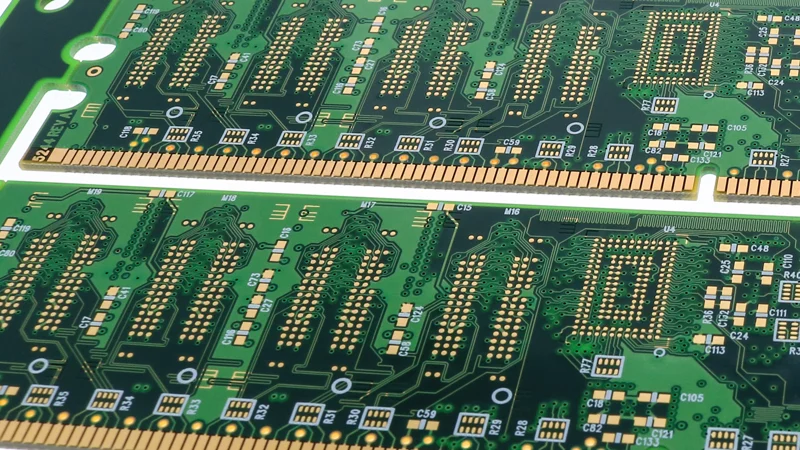
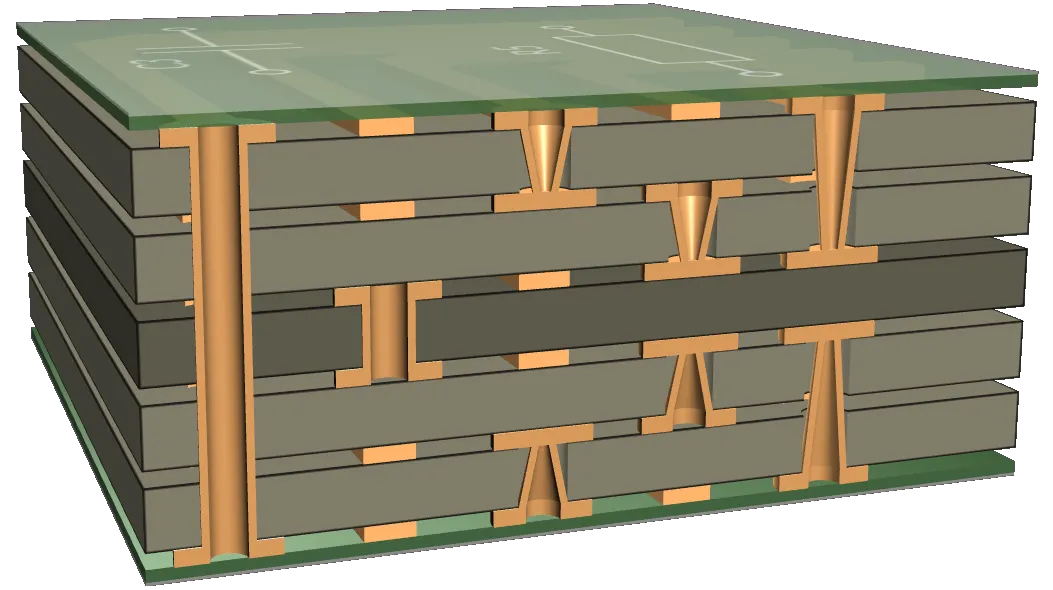
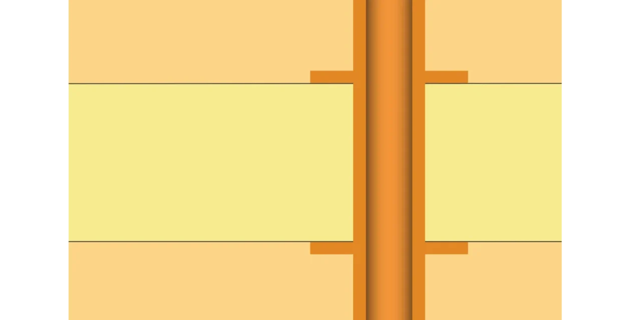
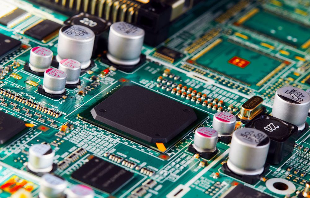
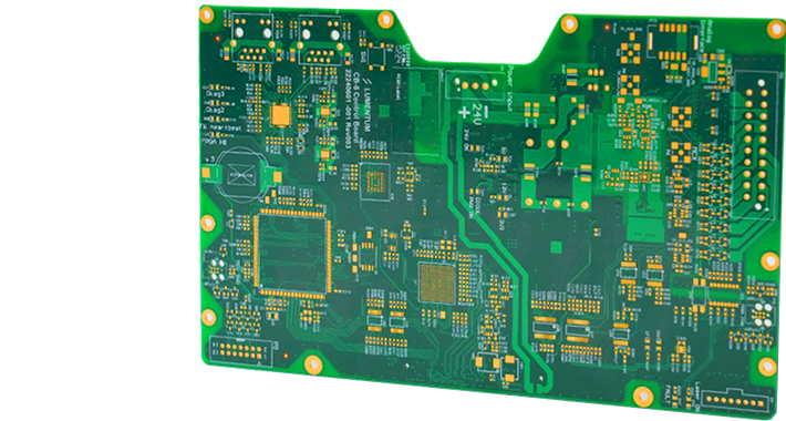
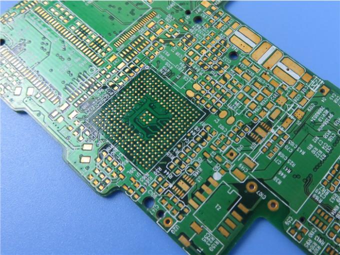
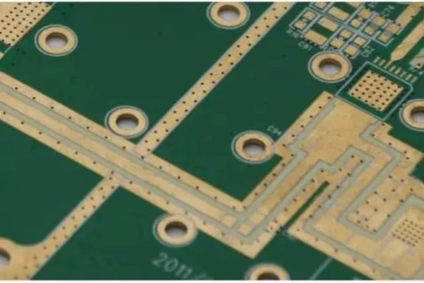
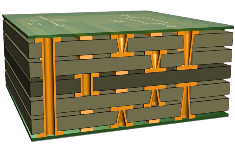
Microvia PCB - KKPCB
 
HomeTag

Microvia PCB - KKPCB

Fine Line PCB: High Precision PCB Manufacturing for HDI and High-Density Routing

What Is a Fine Line PCB? A Fine Line PCB is a high-precision printed circuit board manufactured with ultra-thin trace width and tight trace spacing, enabling high-density routing for advanced electronic products. Compared with standard PCB technology, Fine Line PCB fabrication focuses on achieving smaller line/space (L/S), higher wiring density, and improved signal performance in...

High Frequency Signal PCB: Ensuring Optimal Performance for High-Speed Electronics

What Is a High Frequency Signal PCB? A High Frequency Signal PCB is a printed circuit board specifically engineered to handle high-speed and high-frequency signals with minimal signal loss and optimal signal integrity. These PCBs are crucial in RF communication, 5G modules, high-speed computing, IoT devices, and automotive radar systems. High frequency signals require careful...

Fine Line PCB: Precision Routing for High-Density and High-Speed Electronics

What Is a Fine Line PCB? A Fine Line PCB is a printed circuit board designed with ultra-thin traces and narrow spacing, typically under 4 mils (0.1 mm), enabling high-density interconnections for compact electronic devices. Fine line PCBs are essential in applications where space constraints, high-speed signals, and precise routing are required, such as 5G...

Signal Integrity PCB Design for High-Speed and High-Frequency Electronics

What Is a Signal Integrity PCB? A Signal Integrity PCB is a printed circuit board specifically designed to preserve the quality, timing, and accuracy of electrical signals as they propagate through high-speed and high-frequency circuits. As signal speeds increase and edge rates become faster, maintaining signal integrity (SI) becomes a critical factor in overall system...

Microvia PCB: Advanced HDI PCB Technology for Miniaturized and High-Performance Electronics

Introduction to Microvia PCB A Microvia PCB is a key enabling technology in HDI (High Density Interconnect) PCB manufacturing, designed to meet the increasing demands for miniaturization, high-speed signal transmission, and high component density. By using laser-drilled microvias, Microvia PCBs significantly reduce interconnect length, improve routing flexibility, and enhance overall electrical performance. Microvia PCB technology...

Fine Line PCB: High-Density, Precision PCB Solutions for Advanced Electronics

What Is a Fine Line PCB? A Fine Line PCB is a printed circuit board engineered with ultra-narrow traces and tight spacing, typically below 100 µm. This enables high-density routing and compact component placement while maintaining excellent signal integrity and reliability. Fine line PCBs are essential in high-speed digital systems, RF modules, 5G devices, IoT...

Microvia PCB: Enabling HDI, Miniaturization, and High-Speed Electronic Design

A Microvia PCB is an advanced printed circuit board technology specifically developed for HDI PCB (High Density Interconnect PCB) and high-density PCB applications. By utilizing laser-drilled microvias, Microvia PCBs enable extremely compact routing, superior signal integrity, and reliable interconnections in modern high-speed and high-frequency electronic systems. As electronic products continue to evolve toward miniaturization, higher...

High Reliability PCB: Robust PCB Solutions for Mission-Critical Electronics

A High Reliability PCB is a printed circuit board engineered to maintain consistent electrical and mechanical performance over extended service life, even under harsh environmental and operational conditions. Unlike standard PCBs, high reliability PCBs are designed with enhanced materials, robust structures, and stringent manufacturing controls to meet the demands of mission-critical applications. As electronics are...

Multilayer PCB: Advanced PCB Solutions for High-Density and High-Performance Electronics

A Multilayer PCB is a printed circuit board composed of three or more conductive copper layers laminated together with insulating dielectric materials. Compared to single-layer and double-layer boards, multilayer PCBs offer higher routing density, improved electrical performance, and greater design flexibility, making them essential for modern electronic products. As electronic systems continue to evolve toward...

Low Loss PCB: Advanced PCB Technology for High-Speed, RF, and High-Frequency Applications

A Low Loss PCB is a specialized printed circuit board designed to reduce dielectric loss, insertion loss, and signal distortion in high-speed and high-frequency electronic systems. As modern electronics such as 5G communication systems, RF front-end modules, high-speed data transmission, and semiconductor test equipment operate at ever-increasing frequencies, signal integrity becomes a critical design challenge....