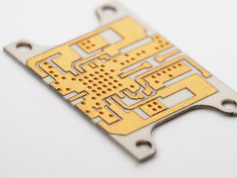
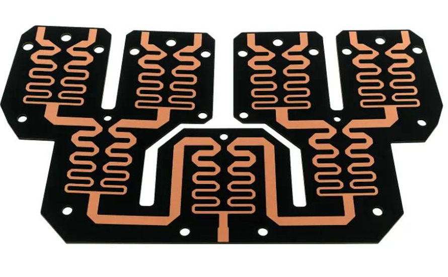
KKPCB - KKPCB
 
HomeTag

KKPCB - KKPCB

PCB Turnkey Services: Streamlining Design, Manufacturing, and Assembly for Faster Time-to-Market

What Is PCB Turnkey? PCB Turnkey refers to a one-stop PCB solution where a single manufacturer manages the entire process—from bare PCB fabrication and electronic component procurement to assembly, testing, and logistics. Instead of coordinating multiple suppliers, customers work with one partner who takes full responsibility for quality, schedule, and delivery. At KKPCB, PCB Turnkey...

From Stackup Planning to Lamination Control: Engineering High Layer Count PCBs That Actually Work

Engineering High Layer Count PCBs: Why “More Layers” Isn’t the Answer As electronic systems evolve toward higher speeds, higher integration, and smaller form factors, high layer count PCBs—typically 16 layers and above—have become standard in data centers, telecommunications, aerospace electronics, and advanced industrial systems. However, many multilayer PCBs fail not because of schematic errors, but...

High-Speed PCB Design & Manufacturing Guide | Signal Integrity, Materials & KKPCB Engineering Capabilities

High-Speed PCB: Engineering Principles, Core Challenges & KKPCB Capabilities High-Speed PCB technology is at the center of every modern data-intensive system—from 5G infrastructure and AI servers to autonomous machines and aerospace communication modules. As signal frequencies climb beyond 3 GHz, 10 GHz, even 28–56 Gbps, traditional PCB design rules become insufficient. High-speed PCB engineering demands...

SiC PCB Engineering: High-Temperature, High-Power, and High-Reliability Solutions for Next-Generation Electronics

Silicon Carbide (SiC) PCBs are rapidly becoming essential for advanced power electronics, electric vehicles, aerospace systems, and industrial automation due to their ability to operate at higher temperatures, voltages, and frequencies than traditional FR-4 or standard ceramic substrates. SiC PCBs integrate wide-bandgap semiconductor technology directly with optimized thermal and electrical performance to support next-generation applications....

Engineering Duroid 6010 PCB for Extreme High-Frequency, Low-Loss, and Ultra-Stable Microwave Applications

As microwave, satellite, radar, and millimeter-wave systems move deeper into high GHz operating regions, engineers require PCB materials with ultra-stable dielectric behavior, extremely high Dk, and exceptionally low loss. This is where Duroid 6010 PCB—based on Rogers RT/duroid® 6010LM—becomes a foundational choice for critical RF and microwave engineering. With a dielectric constant (Dk) of ~10.2,...

Smart Factory PCB Engineering for Intelligent Automation, Real-Time Control, and Industry 4.0 Connectivity

Industrial Automation PCB engineering sits at the core of modern manufacturing, robotics, and process-control systems. In factory environments filled with electrical noise, high temperatures, continuous vibration, and mission-critical timing demands, the Industrial Automation PCB must deliver unwavering reliability, low signal distortion, and stable power delivery. As factories evolve toward smart, interconnected, high-speed architectures, the expectations...

Engineering High Speed PCB for Signal Integrity, Low-Loss Routing, and Next-Generation Data Transmission

As digital systems move toward higher data rates, smaller form factors, and lower power consumption, the demand for High Speed PCB solutions continues to accelerate. From 10–112 Gbps SerDes links to DDR4/DDR5 memory buses and advanced communication modules, a High Speed PCB must deliver loss control, impedance stability, and electromagnetic reliability in increasingly complex environments....

Engineering Double Layer HF PCB for Ultra-Stable RF Performance and Low-Loss Microwave Signal Integrity

As RF communication, IoT edge devices, automotive radar, and compact wireless modules continue to evolve, the Double Layer HF PCB has become a preferred architecture for delivering high-frequency stability, low insertion loss, and predictable electromagnetic performance. Although limited to two copper layers, a Double Layer HF PCB—when engineered correctly—can outperform many multilayer structures in signal...

Unleash Multi-Gigabit Data Fidelity with Precision-Engineered High Speed PCB Architectures for Next-Gen Digital Systems

A High Speed PCB forms the electrical backbone of every modern digital communication system, from multi-gigabit SerDes channels to DDR memory interfaces and high-frequency RF-digital mixed platforms. As data rates continue pushing beyond 10 Gbps, 25 Gbps, and even 56–112 Gbps PAM-4, the engineering demands on a High Speed PCB become far more stringent. Signal...

Achieve Low-Loss Transmission and Stable Impedance Performance with Double Layer HF PCB Engineering for High-Frequency Communication Systems

A Double Layer HF PCB may appear structurally simple, yet in high-frequency engineering it provides a remarkably efficient platform for low-loss propagation, stable impedance, and predictable electromagnetic behavior. When RF designers need high-frequency stability without the cost or stackup escalation of multilayer PCBs, a Double Layer HF PCB offers the ideal balance between manufacturability and...