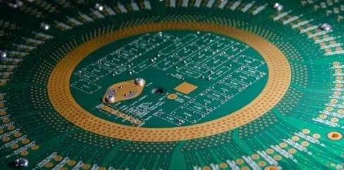
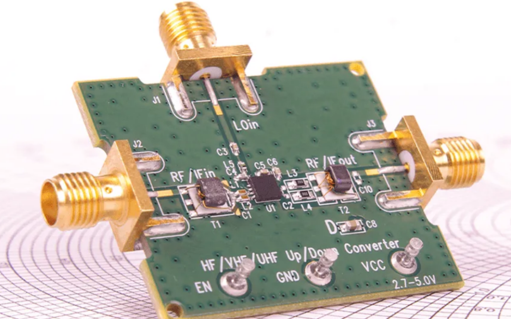
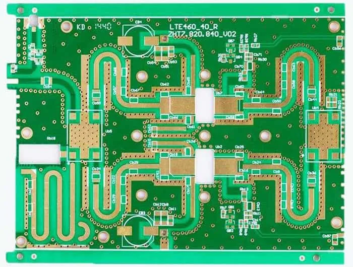
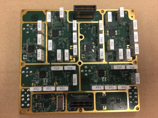
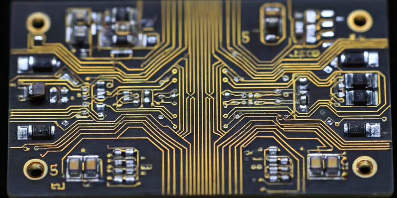
impedance control - KKPCB
 
HomeTag

impedance control - KKPCB

Buy High Frequency PCBs Using Rogers, PTFE, and Hybrid Stackups for High-Speed RF Front-End Modules

As wireless communication, radar systems, and high-speed data transmission continue to advance, high frequency PCBs have become a critical foundation for modern RF front-end modules. Selecting the right materials and stack-up structures—such as Rogers PCBs, PTFE PCBs, and hybrid PCB stackups—is essential to achieving low loss, stable impedance, and reliable RF performance. This article explains...

High-Speed PCB Design & Manufacturing Guide | Signal Integrity, Materials & KKPCB Engineering Capabilities

High-Speed PCB: Engineering Principles, Core Challenges & KKPCB Capabilities High-Speed PCB technology is at the center of every modern data-intensive system—from 5G infrastructure and AI servers to autonomous machines and aerospace communication modules. As signal frequencies climb beyond 3 GHz, 10 GHz, even 28–56 Gbps, traditional PCB design rules become insufficient. High-speed PCB engineering demands...

High Speed PCB Engineering Strategies for Ultra-Reliable, High-Bandwidth, Next-Generation Electronic Systems

A High Speed PCB is no longer a specialty board reserved for telecom giants—it has become the core platform for every high-bandwidth, low-latency, high-frequency electronic architecture. Whether powering 56G/112G SerDes, PCIe 5.0/6.0 interconnects, next-generation routers, AI accelerator hardware, or advanced radar/5G infrastructure, the High Speed PCB defines the system’s ultimate signal integrity, timing accuracy, power...

PCB Prototype Engineering: Achieving High Reliability, High Speed, and High Precision in Modern Electronics

Introduction: Why PCB Prototype Engineering Defines Modern Electronics A PCB Prototype is no longer just a pre-production sample—it is the central engineering stage that determines product performance, manufacturability, reliability, and cost.In advanced electronics such as 5G, IoT, robotics, automotive, aerospace, AI edge computing, and industrial automation, a well-engineered PCB Prototype ensures signal integrity, thermal stability,...

Enhance Electromagnetic Uniformity and Mode-Suppression Using RT/duroid 5880 PCB Stackups in Precision mmWave Routing Networks

Precision mmWave systems increasingly depend on PCB materials that can maintain electromagnetic uniformity, suppress parasitic modes, and control insertion loss across wideband operating ranges. RT/duroid 5880 PCB stackups have become a leading choice for these environments because their low dielectric constant, low-loss tangent, and exceptional stability under thermal and mechanical stress allow engineers to design...

Optimize Dielectric Stability and Low-Df Transmission with Duroid 5880 PCB Architectures for 10–67 GHz RF Subsystems

RF subsystems operating from 10 to 67 GHz—spanning 5G mmWave, satellite links, and aerospace communication modules—demand ultra-stable dielectric properties and minimal signal loss. Any Dk/Df variation or thermal-induced impedance drift directly degrades signal integrity, phase coherence, and overall RF system efficiency. Duroid 5880 PCB laminates (Dk = 2.2 ± 0.02, Df = 0.0009 @10 GHz)...

Minimize Crosstalk and Maintain Impedance Precision Using Advanced Blind Via PCB Layouts in 5G mmWave Systems

5G mmWave hardware doesn’t leave much room for layout mistakes. When operating above 24 GHz, a few microns of misalignment, a poorly shaped via stub, or an uncontrolled dielectric transition can collapse RF integrity. That is why advanced blind via PCB layouts have become a core enabling technology for minimizing crosstalk, stabilizing impedance, and preserving...

Radar PCB Design: Materials, High-Frequency Layout Techniques & Applications

Radar PCB: Design Principles, Materials, Manufacturing Challenges & Key Applications High-speed PCBs stand at the top of modern circuit-board technology, spanning digital high-speed, mixed-signal, and RF/microwave categories. Among these, RF and microwave PCBs operate at the highest frequencies, making them essential for advanced applications—especially RADAR (Radio Detection and Ranging). Because Radar PCBs frequently host a...

WiFi PCB Design Guide for High-Speed Connectivity: Architecture, Materials, RF Layout, and Best Practices

WiFi PCB Design Guide for High-Speed Connectivity Introduction WiFi connectivity is everywhere—from mobile devices to smart home systems and industrial machinery. At the heart of all these wireless systems lies the WiFi PCB, a specialized circuit board engineered to process, transmit, and receive high-frequency wireless signals. This guide explores the structure, design principles, materials, RF...

Hybrid Stackup and Miniaturized RF Design with PTFE PCBs in Next-Generation 5G Base Stations

1. Engineering Overview   Next-generation 5G base stations require high-density, miniaturized RF front-end modules with low insertion loss, precise impedance, and stable phase performance across mmWave bands (28–39 GHz).   PTFE PCB laminates, with Dk = 2.15 ± 0.02 and Df = 0.0009 @10GHz, provide superior dielectric consistency and thermal stability for tightly packed MIMO...