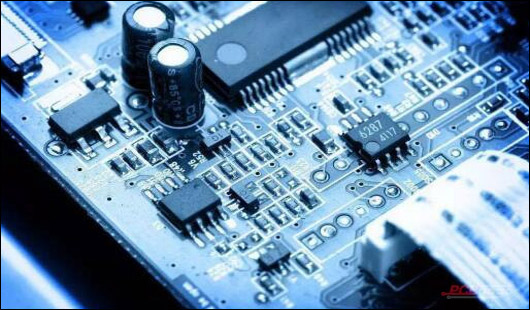
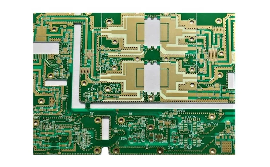
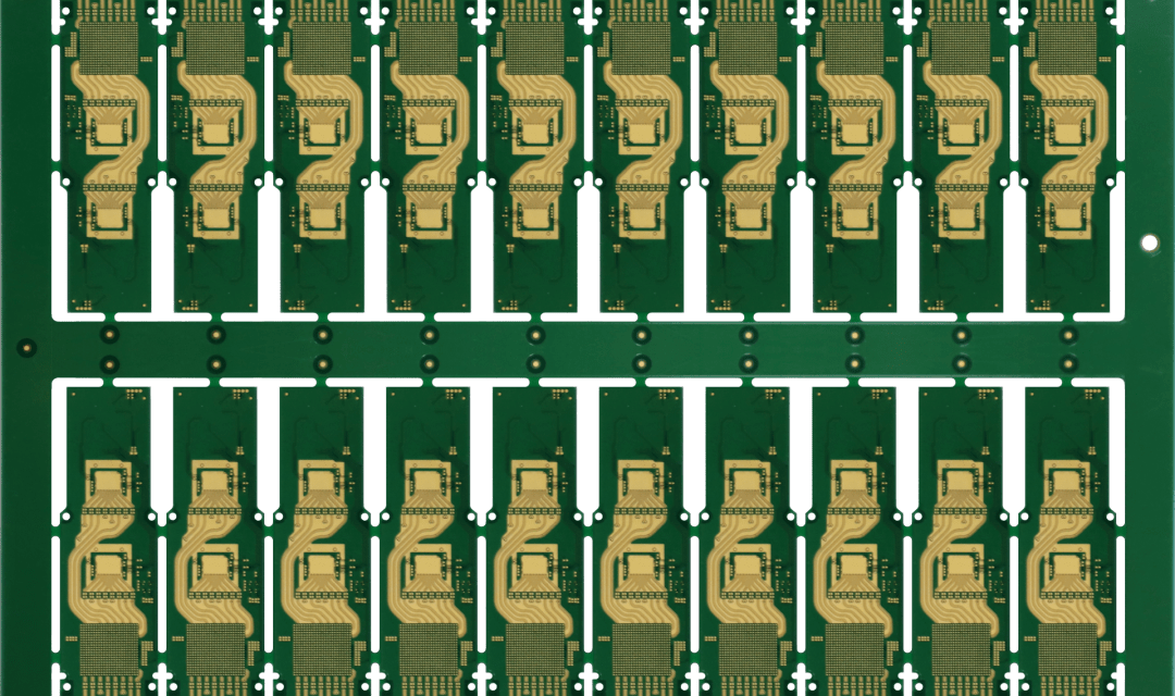
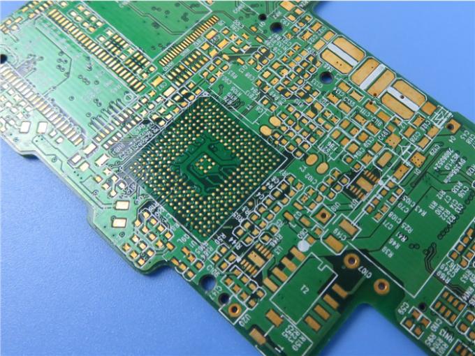
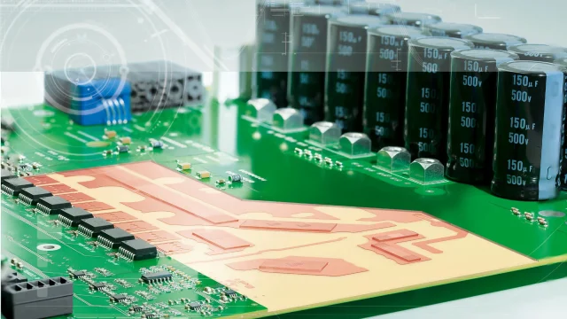
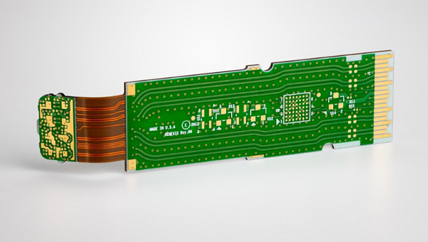
high-speed PCB - KKPCB
 
HomeTag

high-speed PCB - KKPCB

Improve Multi-Gigabit Transmission and Low-Loss Routing Through Impedance Controlled PCB Engineering for Data Center Switches

Modern data center switches demand high-speed, multi-gigabit transmission across densely packed PCB layers. Maintaining low insertion loss, tight impedance control, and minimal crosstalk is critical to guarantee reliable signal integrity, reduce latency, and preserve network throughput. Impedance-controlled PCB architectures provide predictable high-frequency performance for differential pair routing and dense multilayer stackups. KKPCB leverages precision lamination,...

Maximize RF Channel Integrity and Minimize Signal Loss with Blind Via PCB Architectures for High-Speed Communication Modules

High-speed communication modules in 5G, satellite transceivers, and high-frequency computing systems demand extreme precision in signal routing and interconnect integrity. As layer density increases and modules become more compact, traditional through-hole vias introduce unwanted parasitic effects, signal reflection, and EMI interference, compromising both channel fidelity and system performance. Blind via PCB technology enables selective inter-layer...

Achieve Multi-Gig Channel Reliability and Tight Impedance Control with Megtron 7 PCB Stackups for Advanced Server Motherboards

Modern server motherboards require predictable impedance, extremely low jitter, and stable multi-gigabit routing to support DDR5, PCIe 6.0, and high-density network interfaces. FR-4-class materials fail to provide consistent loss and dielectric stability. Megtron 7 PCB laminates supply ultra-low Df, tight dielectric tolerances, and high-temperature reliability suited for 8–64 GT/s environments. KKPCB adapts Megtron 7 PCB...

Enhance High-Speed Signal Integrity and Low-Loss Performance with Megtron 7 PCB Platforms for 112G/224G SerDes Systems

Next-generation 112G/224G SerDes channels push FR-4 far beyond its electrical limits. As data center switching, AI computing, and PCIe-6/7 architectures scale upward, loss tangent, copper roughness, and impedance drift become critical bottlenecks. Megtron 7 PCB laminates—Df 0.0012 class, highly stable Dk, and low copper-permittivity interaction—provide an electrically clean foundation for long-reach PAM4 channels. KKPCB integrates...

High-Frequency Signal Integrity Optimization and Phase-Stable Transmission with Megtron 7 PCB Substrates in 5G Server and High-Speed Computing Systems

Megtron 7 PCB laminates are widely adopted in 5G servers, AI computing accelerators, and cloud networking equipment due to their exceptionally low dielectric loss and superior stability at 28–112 Gbps PAM4 and mmWave bands. As system architectures transition toward high-density multi-lane SerDes and advanced RF interconnects, PCB materials become a primary constraint influencing channel loss...

Low Loss PCBs Explained: Materials, Features & High-Frequency Performance

What Is a Low Loss PCB? Premium Materials, Performance Advantages & Applications In high-frequency electronics, signal integrity is everything. As data rates climb and RF systems move into the mmWave range, traditional FR-4 PCBs quickly become inadequate due to excessive dielectric loss, copper loss and thermal instability. At KKPCB, we engineer Low Loss PCBs specifically...

WiFi PCB Design Guide for High-Speed Connectivity: Architecture, Materials, RF Layout, and Best Practices

WiFi PCB Design Guide for High-Speed Connectivity Introduction WiFi connectivity is everywhere—from mobile devices to smart home systems and industrial machinery. At the heart of all these wireless systems lies the WiFi PCB, a specialized circuit board engineered to process, transmit, and receive high-frequency wireless signals. This guide explores the structure, design principles, materials, RF...

Enhancing Signal Integrity and Crosstalk Control of Megtron 6 PCBs in High-Speed 5G Smartphone Processor Boards

1. Engineering Overview   As 5G smartphone processors integrate multiple high-speed RF and data lanes within increasingly compact layouts, signal integrity and crosstalk control have become critical design challenges. Crosstalk between closely spaced differential pairs can induce timing errors and reduce data fidelity. Megtron 6 PCBs, with their stable dielectric constant (Dk = 3.45 ±0.02)...

Mastering High-Speed PCB Test Point Design: Precision, Performance, and Signal Integrity

Mastering High-Speed PCB Test Point Design: Precision, Performance, and Signal Integrity In high-speed printed circuit board (PCB) design, test point placement is far more than a routine step—it’s a science of balance. The miniature metal pads scattered across a PCB may look simple, but their position, size, and electrical behavior can determine whether a product...