high-speed PCB - KKPCB
 
HomeTag

high-speed PCB - KKPCB

Signal Integrity PCBs: Optimized for High-Speed and High-Fidelity Electronics

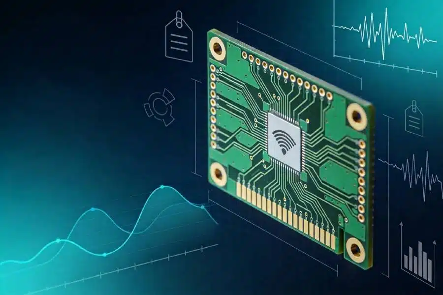
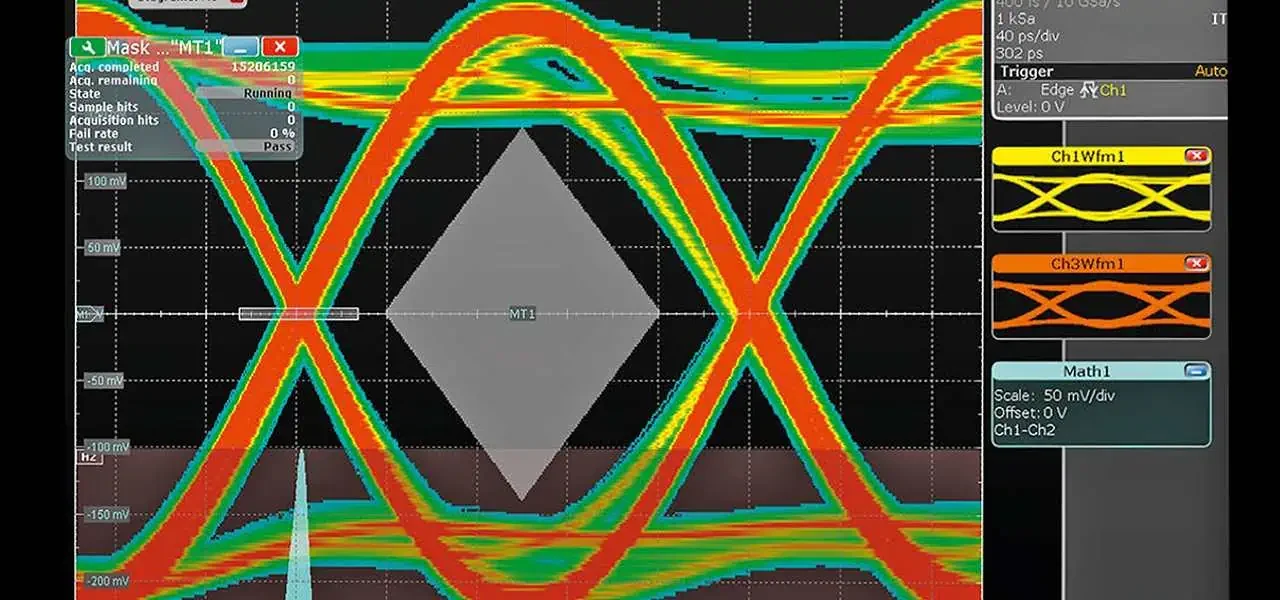
What is a Signal Integrity PCB? A Signal Integrity (SI) PCB is a printed circuit board designed to maintain high-fidelity signal transmission in high-speed digital, RF, or mixed-signal systems. Unlike conventional PCBs, SI PCBs focus on minimizing signal degradation, reflections, crosstalk, and timing errors, ensuring that signals arrive accurately at their destinations. Signal integrity is...

Megtron PCBs: Advanced Low-Loss Solutions for High-Speed Applications

What is a Megtron PCB? A Megtron PCB is a printed circuit board built using Megtron high-frequency laminates, developed to provide low dielectric loss (Df), stable dielectric constant (Dk), and excellent thermal performance for high-speed and high-frequency electronics. Megtron laminates are commonly used in: High-speed communication devices RF and microwave circuits Gigabit and multi-gigabit data...

High Frequency Laminates: Key Materials for Advanced PCB Performance

What is a High Frequency Laminate PCB? A High Frequency Laminate PCB is a printed circuit board built with specialized substrate materials optimized for low dielectric loss (Df), stable dielectric constant (Dk), and high thermal performance at high frequencies. Unlike standard FR-4, high frequency laminates maintain signal integrity in RF, microwave, and high-speed digital applications,...

PTFE PCBs: Ultra-Low Loss Solutions for High-Frequency Electronics

What is a PTFE PCB? A PTFE PCB is a printed circuit board built using polytetrafluoroethylene (PTFE) as the substrate. PTFE is a high-performance polymer renowned for its extremely low dielectric loss (Df), consistent dielectric constant (Dk), and high thermal stability. These characteristics make PTFE PCBs ideal for applications where high-frequency signal integrity and minimal...

Fine Line PCBs: Precision Manufacturing for Ultra-High-Density Electronics

What is a Fine Line PCB? A Fine Line PCB is a printed circuit board designed with extremely narrow trace widths and spacing, typically below 100 microns. These PCBs are essential for high-density electronic designs where space is limited and performance requirements are demanding. Fine line technology is widely used in applications that require compact...

Microvia PCBs: Enabling High-Density and High-Performance Electronics

What is a Microvia PCB? A Microvia PCB is a printed circuit board that uses very small vias—typically less than 150 microns in diameter—to connect adjacent layers. Unlike traditional through-hole or buried vias, microvias enable high-density routing and reduced signal path lengths, making them ideal for high-speed, high-performance, and compact electronic designs. Microvia technology is...

Fine Pitch PCBs: Precision Design for High-Density Components

As electronic devices become smaller and more powerful, the demand for Fine Pitch PCBs—boards designed for components with extremely small pin spacing—has grown significantly. Fine pitch components, such as BGA, QFN, and CSP packages, require precise PCB design and manufacturing to ensure electrical connectivity, signal integrity, and long-term reliability. Design Considerations High-Density Layouts:Fine pitch PCBs...

Custom ATE PCBs: Precision Design for Automated Test Equipment

Automated Test Equipment (ATE) plays a vital role in validating electronic components, modules, and systems. At the heart of these test platforms are Custom ATE PCBs, engineered to handle high-speed signals, precise routing, and repeated testing cycles without failure. These PCBs must balance electrical performance, mechanical stability, and long-term reliability to meet stringent testing requirements....

HDI PCBs: Unlocking High-Density Performance for Modern Electronics

High-Density Interconnect (HDI) PCBs are a key technology for today’s compact and high-performance electronics. With fine lines, microvias, blind and buried vias, and multiple layers, HDI PCBs allow designers to fit complex circuits into small form factors, supporting applications from mobile devices to 5G infrastructure, automotive electronics, aerospace systems, and industrial IoT devices. Advanced Design...

Buried Via PCB: Advanced Multilayer Interconnects for High-Density Electronics

As electronic devices become smaller and more complex, the need for high-density interconnections within printed circuit boards increases. Buried via PCBs offer a solution by connecting inner layers without using surface space, allowing for compact, high-performance multilayer boards. Buried vias improve routing flexibility, signal integrity, and design density, making them critical for advanced applications such...