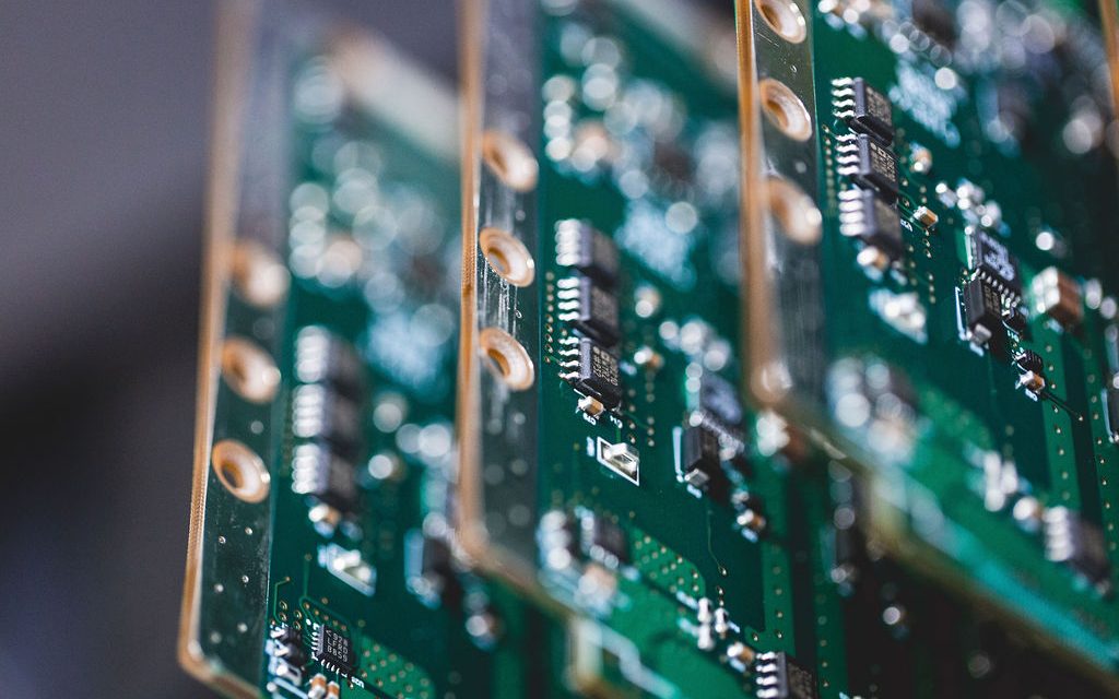
high-speed PCB - KKPCB
 
HomeTag

high-speed PCB - KKPCB

Professional High Frequency PCB OEM for RF and High-Speed Communication Systems

With the rapid evolution of RF, microwave, and high-speed communication technologies, PCB performance has become a critical factor in system reliability and signal integrity. Selecting a professional high frequency PCB OEM is essential for manufacturers developing RF and high-speed communication systems that operate in GHz and millimeter-wave environments. A qualified high frequency PCB OEM combines...

High Frequency PCB Manufacturer: Precision Manufacturing for RF, Microwave, and High-Speed Applications

As wireless communication, 5G, radar, and high-speed electronics continue to evolve, the demand for a reliable high frequency PCB manufacturer has increased significantly. High frequency PCBs operate in GHz and millimeter-wave ranges, where signal integrity, material stability, and manufacturing precision are critical. This article explains what defines a high frequency PCB manufacturer, the key capabilities...

High Frequency PCB Supplier: How to Choose a Reliable Partner for RF and Microwave Applications

As electronic systems continue to move toward higher speeds and higher frequencies, selecting the right high frequency PCB supplier has become critical for RF, microwave, and millimeter-wave applications. High frequency PCBs require specialized materials, tight impedance control, and advanced manufacturing processes to ensure stable signal performance. This article outlines what defines a qualified high frequency...

High Frequency PCB Manufacturer: How to Choose the Right Partner for RF & Microwave Applications

In high-speed communications, radar systems, 5G infrastructure, and other cutting-edge electronics, the role of a high frequency PCB manufacturer is more important than ever. High frequency PCBs operate at gigahertz (GHz) and millimeter-wave frequencies, requiring precision design, specialized materials, and advanced fabrication techniques that differ significantly from standard PCB production. Selecting the right manufacturer influences...

Buy High Frequency PCBs Using Rogers, PTFE, and Hybrid Stackups for High-Speed RF Front-End Modules

As wireless communication, radar systems, and high-speed data transmission continue to advance, high frequency PCBs have become a critical foundation for modern RF front-end modules. Selecting the right materials and stack-up structures—such as Rogers PCBs, PTFE PCBs, and hybrid PCB stackups—is essential to achieving low loss, stable impedance, and reliable RF performance. This article explains...

Accelerate Product Validation and Engineering Iteration with High-Reliability Small Batch PCB Manufacturing

In today’s highly competitive electronics market, speed and reliability are critical during the product development stage. High-reliability small batch PCB manufacturing enables engineers to accelerate product validation, shorten engineering iteration cycles, and reduce development risk before mass production. This article explains how small batch PCB manufacturing supports rapid prototyping, design verification, and engineering optimization, helping...

Impedance Control on PCBs: Why It Matters for High-Speed, RF, and High-Frequency Circuit Design

As electronic devices continue to evolve toward higher speeds, greater bandwidth, and higher operating frequencies, impedance control on PCBs has become a critical requirement rather than an optional design consideration. In high-speed PCB, RF PCB, and high-frequency circuit design, improper impedance control can lead to signal degradation, EMI issues, and overall system instability. This article...

Designing Buried Via PCBs for High-Density Routing and Signal Integrity Optimization

As electronic systems continue to evolve toward higher speed, smaller form factors, and increased functionality, traditional through-hole via structures are becoming a limiting factor. Buried Via PCB technology has emerged as a critical enabler for high-density routing and signal integrity optimization, particularly in HDI, high-speed digital, and RF applications. By embedding vias between inner layers...

From Stackup Planning to Lamination Control: Engineering High Layer Count PCBs That Actually Work

Engineering High Layer Count PCBs: Why “More Layers” Isn’t the Answer As electronic systems evolve toward higher speeds, higher integration, and smaller form factors, high layer count PCBs—typically 16 layers and above—have become standard in data centers, telecommunications, aerospace electronics, and advanced industrial systems. However, many multilayer PCBs fail not because of schematic errors, but...

Balancing Electrical Performance and Manufacturability in Buried Via PCB Structures

As electronic systems continue to evolve toward higher speeds, greater functionality, and reduced form factors, Buried Via PCB structures have become a critical enabler for advanced multilayer designs. By allowing interlayer connections without penetrating the outer layers, buried vias unlock higher routing density, improved signal integrity, and enhanced EMI control. However, these electrical advantages must...