High Layer Count PCB - KKPCB
 
HomeTag

High Layer Count PCB - KKPCB

Fine Pitch PCB – Precision PCB for High Density and Fine Line Applications

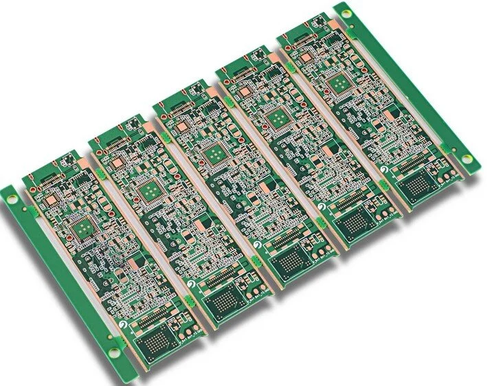
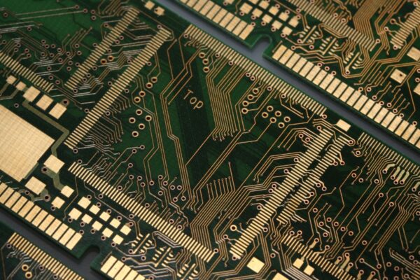
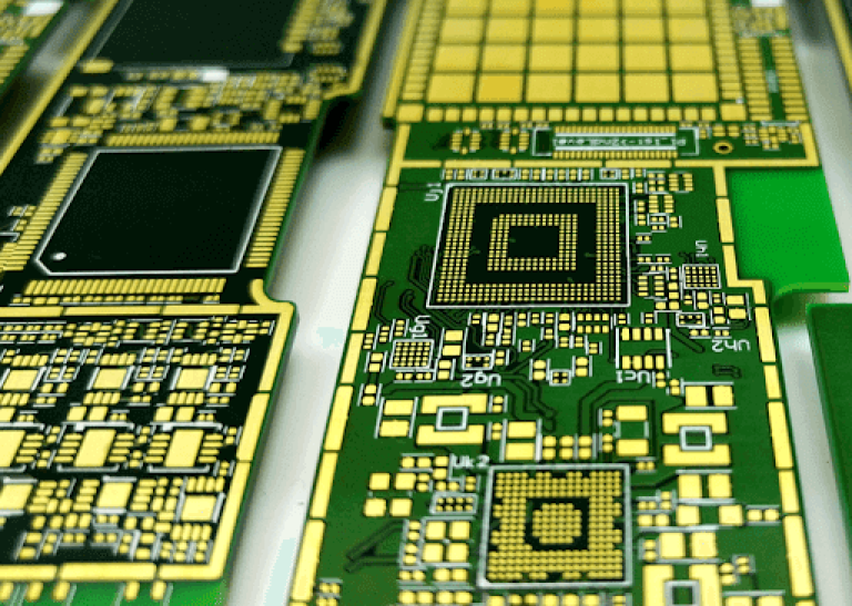
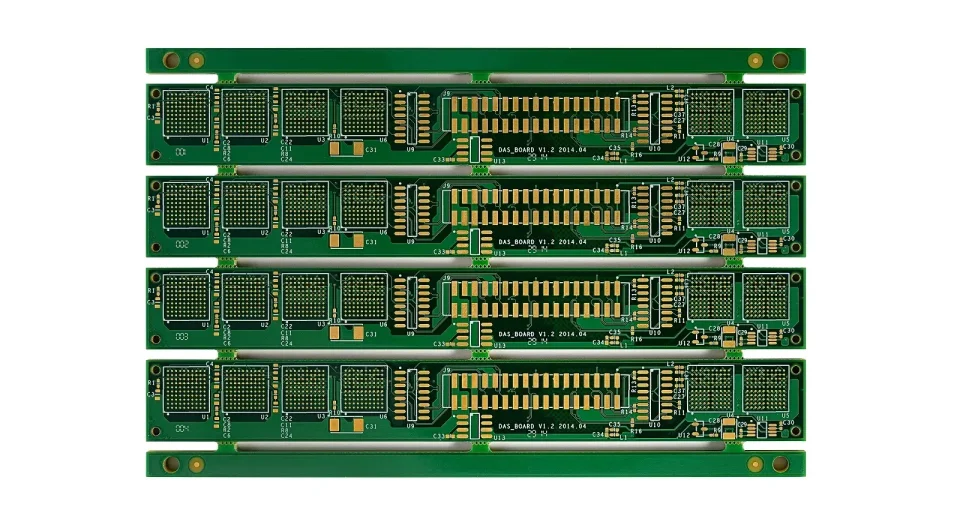
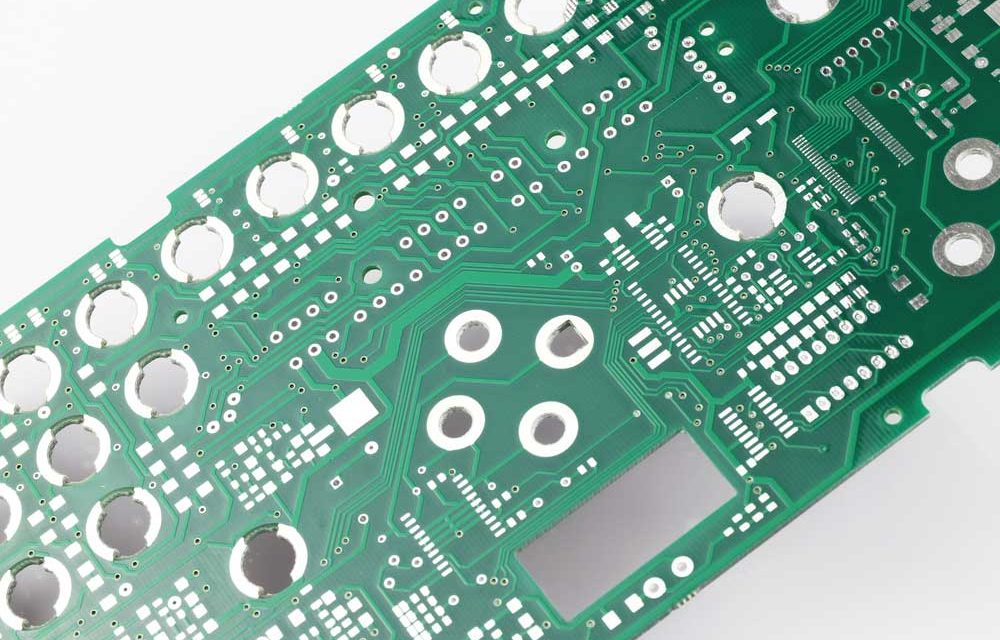
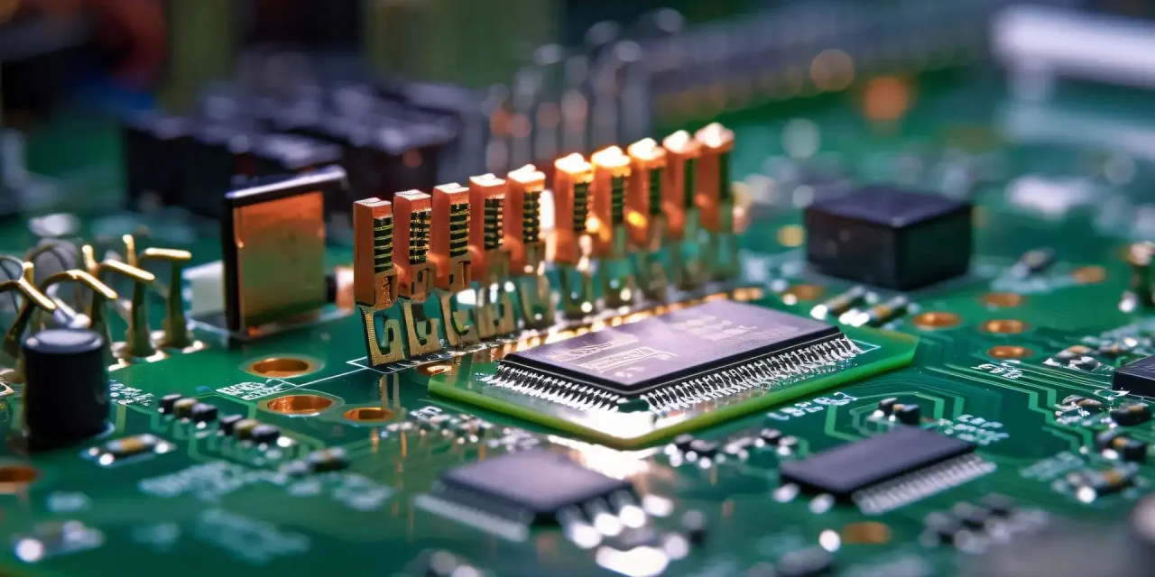
What Is Fine Pitch PCB? A Fine Pitch PCB refers to a printed circuit board designed with extremely small trace width and spacing to support high pin count and fine pitch components. It is commonly used in advanced electronic systems where compact design, high integration, and precise routing are essential. Fine pitch designs are typically...

HDI PCB – High Density Interconnect PCB for Advanced Electronics

What Is HDI PCB? HDI PCB (High Density Interconnect PCB) is a printed circuit board designed with higher wiring density per unit area compared to traditional multilayer PCBs. It uses advanced manufacturing technologies such as microvias, blind vias, buried vias, and fine line traces to achieve compact size and improved electrical performance. HDI PCB is...

ATE Test PCB – High Precision PCB for Automated Test Equipment Applications

What Is an ATE Test PCB? An ATE Test PCB is a specialized printed circuit board designed for use in Automated Test Equipment (ATE) systems. It acts as the electrical interface between semiconductor devices and the test platform, enabling accurate signal transmission, power delivery, and measurement during IC testing. ATE Test PCB is commonly used...

Buried Via PCB – Advanced Multilayer PCB with Internal Interconnection Technology

What Is a Buried Via PCB? A Buried Via PCB is a multilayer printed circuit board that contains vias connecting internal layers only, without reaching the outer surface layers. Unlike through-hole vias, buried vias are completely enclosed within the board stack-up. This allows designers to: Increase routing density Optimize outer layer space Improve signal integrity...

High Layer Count PCB – Advanced Multilayer PCB for High Density and High Speed Applications

What Is a High Layer Count PCB? A High Layer Count PCB refers to a multilayer printed circuit board typically built with 16 layers or more, and in advanced applications, up to 40, 60, or even higher layer counts. High Layer Count PCB is designed to support: High density routing Complex signal distribution Controlled impedance...

Satellite PCB – High Reliability PCB for Space and Satellite Communication Systems

What Is a Satellite PCB? A Satellite PCB is a high reliability printed circuit board engineered for space and satellite communication systems. These PCBs are designed to operate in: Extreme temperature fluctuations High radiation environments Vacuum conditions High vibration and launch shock Satellite PCB must provide long-term reliability, stable signal transmission, and mechanical integrity, as...

Blind Via PCB – High Density Interconnect PCB for Compact and High Speed Designs

What Is a Blind Via PCB? A Blind Via PCB is a type of printed circuit board that contains vias connecting internal layers to one or more outer layers without passing completely through the board. Unlike through-hole vias, blind vias help: Reduce board size Increase routing density Optimize multilayer stack-ups Support HDI (High Density Interconnect)...

Impedance Controlled PCB – High Precision PCB for High Speed Signal Integrity

What Is an Impedance Controlled PCB? An Impedance Controlled PCB is a printed circuit board designed to maintain precise characteristic impedance along signal traces. This is critical for high speed digital circuits, RF communication, and microwave systems, where mismatched impedance can cause: Signal reflection Crosstalk Data errors Timing skew Impedance control ensures reliable signal integrity...

High Layer Count PCB for Complex and High-Density Electronic Systems

What Is a High Layer Count PCB? A High Layer Count PCB refers to a multilayer printed circuit board containing a large number of copper layers, typically 12 layers and above, designed to support highly complex circuit routing and high-speed signal transmission. High Layer Count PCBs are widely used in advanced electronic systems that require...

ATE PCB Supplier Capabilities for High-Speed, High-Reliability Automated Test Equipment Systems

An ATE PCB supplier is a critical technical partner in the development of Automated Test Equipment (ATE) systems used for semiconductor validation, characterization, and production testing. Unlike general-purpose electronics, ATE platforms demand extreme electrical accuracy, mechanical durability, and long-term repeatability, placing significantly higher requirements on PCB design and manufacturing quality. Technical Demands of ATE PCB...