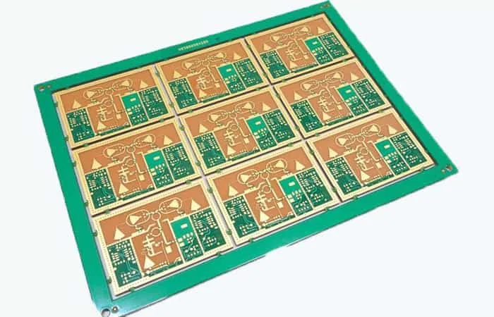
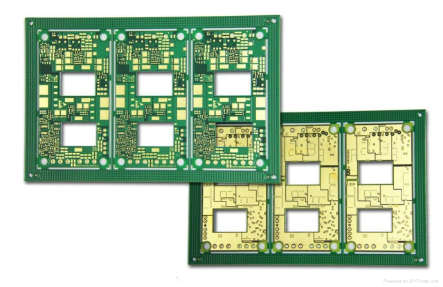
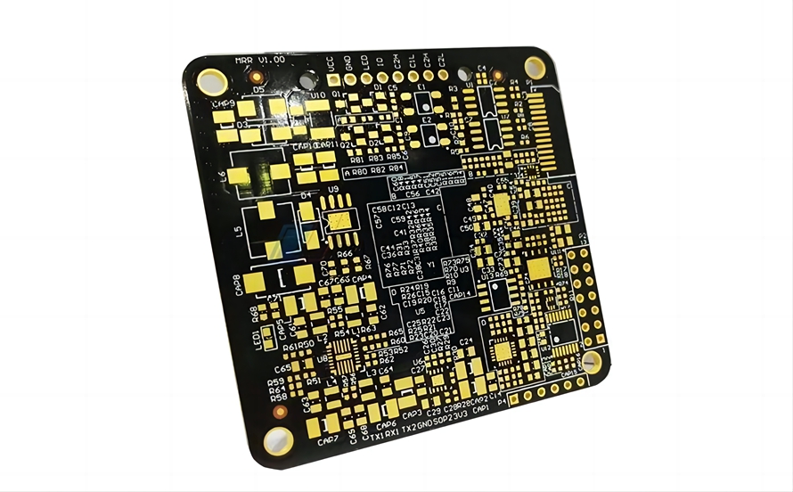
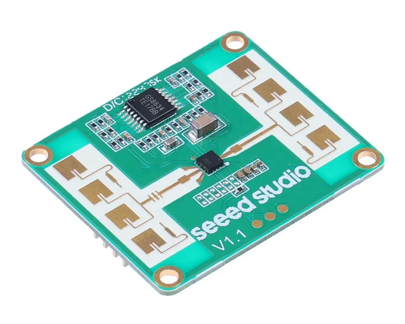
high-frequency PCB - KKPCB
 
HomeTag

high-frequency PCB - KKPCB

mmWave Module PCB Engineering for High-Frequency, Low-Loss and Thermally Stable RF Front-End Systems

The shift toward 5G FR2, advanced radar, high-resolution sensing and satellite communication has placed intense performance pressure on mmWave Module PCB design. At frequencies from 24 GHz to 86 GHz, the PCB is no longer a passive carrier—it becomes an active RF component whose materials, stackup, via transitions and routing geometries directly dictate performance. A...

Boost Multi-Sensor Processing Efficiency Using High-Density UAV PCB Designs in Intelligent Aerial Surveillance Platforms

In next-generation intelligent aerial surveillance platforms, UAV manufacturers face increasing demands for real-time data fusion, long-range imaging, high-throughput RF links, and multi-sensor synchronization. These requirements place enormous pressure on the UAV PCB architecture, especially in compact airframes where thermal, mechanical, and electromagnetic constraints are all tightly coupled. This is why high-density PCB design (HDI PCB),...

Maximize RF Power Handling and Phase Stability Using RO4350B PCB Laminates in High-Frequency Antenna Modulegs

Modern wireless systems—from 5G radio units and phased-array antenna modules to automotive radar and satellite communication terminals—demand PCBs that deliver high RF power handling, exceptional phase stability, and ultra-low loss. As antenna modules continue to shrink while operating at higher frequencies, selecting the correct laminate becomes a mission-critical design decision. Among all mid-frequency RF substrates,...

Enhance Signal Integrity and Thermal Reliability in Multilayer Blind Via PCBs for High-Density RF Modules

High-density RF modules in 5G base stations, satellite payloads, and advanced IoT systems require compact multilayer PCBs with precise signal routing, minimal crosstalk, and high thermal resilience. Blind via technology allows for efficient vertical interconnects while reducing PCB stackup thickness, improving high-frequency performance, and maintaining signal integrity across densely packed layers. KKPCB integrates precision lamination,...

Reduce Insertion Loss and Enhance Power Efficiency Using Low Loss PCB Designs for Satellite Communication Payloads

Satellite communication payloads demand high-frequency RF stability, minimal insertion loss, and optimized power efficiency across densely packed multilayer PCBs. Signal integrity degradation, EMI coupling, or thermal hotspots can compromise link margin, telemetry accuracy, and antenna performance. Low loss PCB materials, such as ceramic-reinforced laminates or PTFE-based RF substrates, provide stable dielectric constant (Dk) and low...

Optimize Phase-Stable High-Frequency Routing with Blind Via PCB Architectures in Compact Satellite Communication Payloads

Compact satellite communication payloads require precise, phase-stable RF routing to maintain signal fidelity and low insertion loss across high-frequency channels. The limited space and high-density requirements make blind via architectures essential for multilayer PCBs, enabling signal interconnects without penetrating all layers, reducing parasitic capacitance, and controlling crosstalk. Blind via PCBs allow compact routing of RF...

Optimize Beamforming Accuracy and Ultra-Low-Loss RF Propagation Using High-Frequency mmWave Module PCB Architectures for 28–60 GHz Wireless Platforms

High-frequency mmWave module PCB architectures define the performance boundary of 28–60 GHz wireless platforms, where beamforming accuracy, ultra-low-loss routing, and tight impedance control determine every detail of system efficiency. In dense phased-array units, even microscopic changes in Dk/Df, copper roughness, dielectric uniformity, or via transition geometry produce measurable degradation in beam steering vectors, noise floors,...

Minimize Crosstalk and Maintain Impedance Precision Using Advanced Blind Via PCB Layouts in 5G mmWave Systems

5G mmWave hardware doesn’t leave much room for layout mistakes. When operating above 24 GHz, a few microns of misalignment, a poorly shaped via stub, or an uncontrolled dielectric transition can collapse RF integrity. That is why advanced blind via PCB layouts have become a core enabling technology for minimizing crosstalk, stabilizing impedance, and preserving...

Unlock Ultra-Stable RF Propagation and Low-Loss Routing with Next-Gen Multilayer HF PCB Platforms for Dense mmWave Arrays

Dense mmWave arrays, commonly used in 5G massive MIMO, radar, and satellite phased arrays, require ultra-stable RF propagation, minimal insertion loss, and precise impedance control across multilayer interconnects. Thermal stress, mechanical vibration, and high-frequency crosstalk can severely degrade signal fidelity, phase alignment, and overall array performance. Next-generation multilayer HF PCB platforms leverage advanced dielectric laminates...

Optimize High-Frequency UAV PCB Architectures to Enhance IoT Crop Monitoring, Precision Spraying, and Long-Range Agricultural Drone Communication

IoT-enabled agricultural UAVs operate in a uniquely demanding environment: wide temperature swings, continuous vibration, variable humidity, and rapidly changing RF propagation conditions over open farmland. These drones must maintain long-range wireless links, collect high-resolution crop data, and execute precision-controlled spraying while keeping power consumption and mass as low as possible. To meet these requirements, modern...