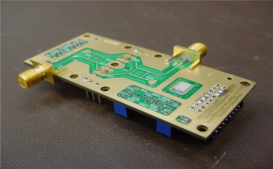
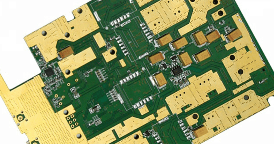
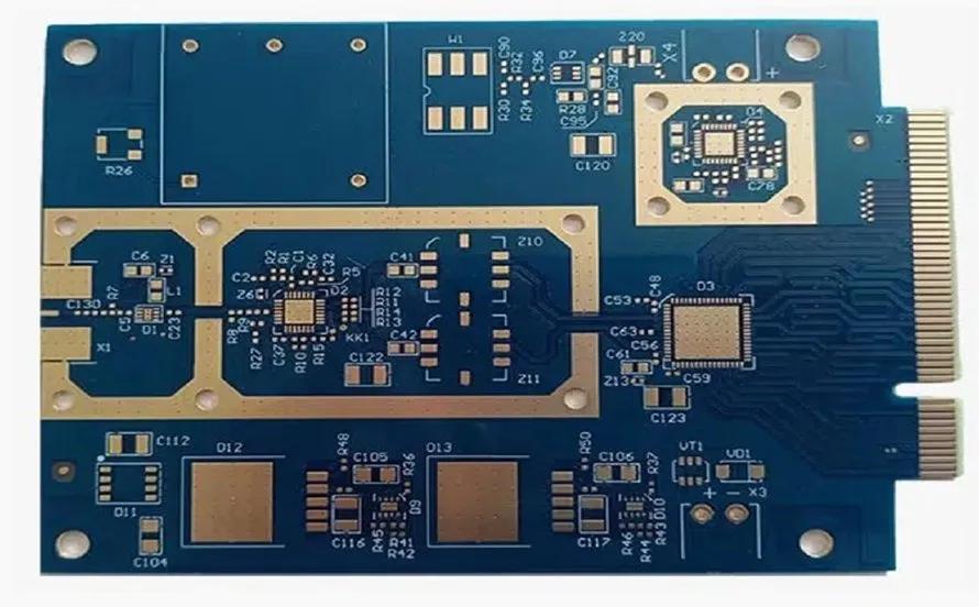
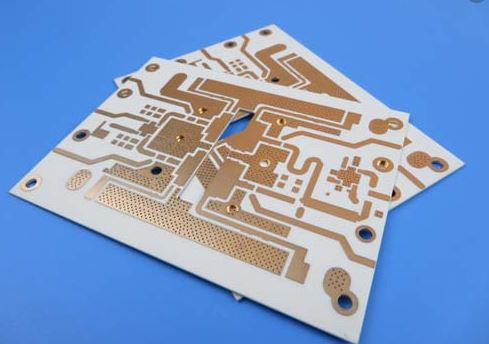
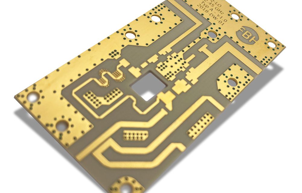
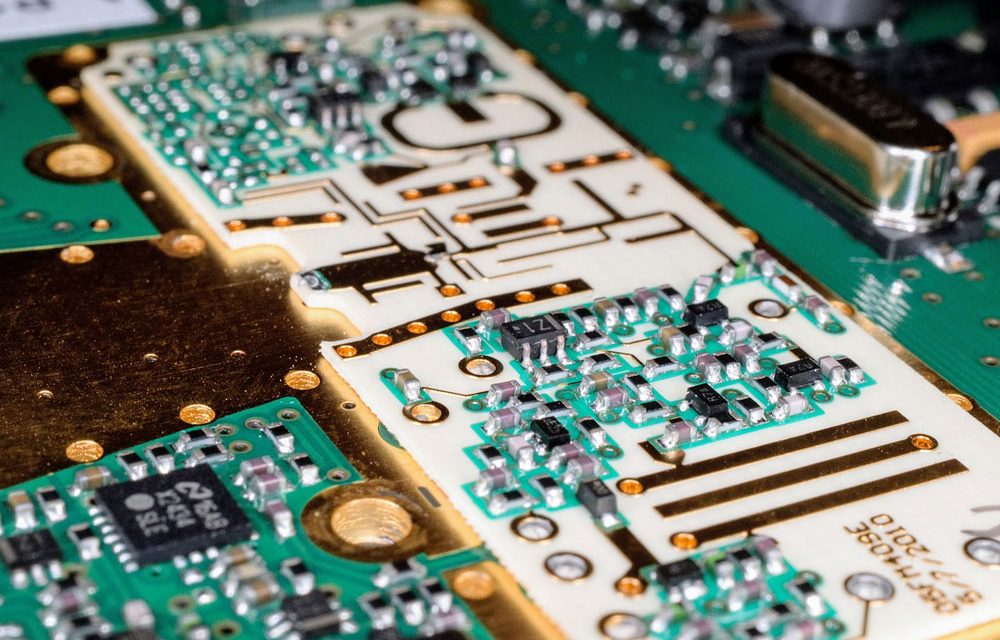
high-frequency PCB - KKPCB
 
HomeTag

high-frequency PCB - KKPCB

Reduce Insertion Loss and Enhance Power Efficiency Using Low Loss PCB Designs for Satellite Communication Payloads

Satellite communication payloads demand high-frequency RF stability, minimal insertion loss, and optimized power efficiency across densely packed multilayer PCBs. Signal integrity degradation, EMI coupling, or thermal hotspots can compromise link margin, telemetry accuracy, and antenna performance. Low loss PCB materials, such as ceramic-reinforced laminates or PTFE-based RF substrates, provide stable dielectric constant (Dk) and low...

Optimize Phase-Stable High-Frequency Routing with Blind Via PCB Architectures in Compact Satellite Communication Payloads

Compact satellite communication payloads require precise, phase-stable RF routing to maintain signal fidelity and low insertion loss across high-frequency channels. The limited space and high-density requirements make blind via architectures essential for multilayer PCBs, enabling signal interconnects without penetrating all layers, reducing parasitic capacitance, and controlling crosstalk. Blind via PCBs allow compact routing of RF...

Optimize Beamforming Accuracy and Ultra-Low-Loss RF Propagation Using High-Frequency mmWave Module PCB Architectures for 28–60 GHz Wireless Platforms

High-frequency mmWave module PCB architectures define the performance boundary of 28–60 GHz wireless platforms, where beamforming accuracy, ultra-low-loss routing, and tight impedance control determine every detail of system efficiency. In dense phased-array units, even microscopic changes in Dk/Df, copper roughness, dielectric uniformity, or via transition geometry produce measurable degradation in beam steering vectors, noise floors,...

Minimize Crosstalk and Maintain Impedance Precision Using Advanced Blind Via PCB Layouts in 5G mmWave Systems

5G mmWave hardware doesn’t leave much room for layout mistakes. When operating above 24 GHz, a few microns of misalignment, a poorly shaped via stub, or an uncontrolled dielectric transition can collapse RF integrity. That is why advanced blind via PCB layouts have become a core enabling technology for minimizing crosstalk, stabilizing impedance, and preserving...

Unlock Ultra-Stable RF Propagation and Low-Loss Routing with Next-Gen Multilayer HF PCB Platforms for Dense mmWave Arrays

Dense mmWave arrays, commonly used in 5G massive MIMO, radar, and satellite phased arrays, require ultra-stable RF propagation, minimal insertion loss, and precise impedance control across multilayer interconnects. Thermal stress, mechanical vibration, and high-frequency crosstalk can severely degrade signal fidelity, phase alignment, and overall array performance. Next-generation multilayer HF PCB platforms leverage advanced dielectric laminates...

Optimize High-Frequency UAV PCB Architectures to Enhance IoT Crop Monitoring, Precision Spraying, and Long-Range Agricultural Drone Communication

IoT-enabled agricultural UAVs operate in a uniquely demanding environment: wide temperature swings, continuous vibration, variable humidity, and rapidly changing RF propagation conditions over open farmland. These drones must maintain long-range wireless links, collect high-resolution crop data, and execute precision-controlled spraying while keeping power consumption and mass as low as possible. To meet these requirements, modern...

Boost RF Linearity and Phase Consistency with Impedance Controlled PCB Architectures in Aerospace Navigation and Telemetry Modules

Aerospace navigation and telemetry links depend on signals that simply cannot drift, distort, or wander off-phase. Whether guiding a launch vehicle or stabilizing a satellite’s inter-orbital communication, the RF path must maintain tight impedance control, predictable phase behavior, and ultra-low distortion across multi-GHz carriers. This is where Impedance Controlled PCB architectures become fundamental—not an optional...

Achieve Low-Loss Performance and Long-Term Stability Through ADAS PCB Materials for Multi-Sensor Fusion Modules

Advanced driver-assistance systems (ADAS) rely heavily on multi-sensor fusion, where radar, LiDAR, ultrasonic sensing, and camera modules continuously exchange high-frequency data. To maintain real-time performance and safety-critical reliability, the ADAS PCB must deliver low-loss signal transmission, stable dielectric behavior, and tight impedance control under prolonged automotive thermal and vibration stress. High-frequency ADAS RF chains—particularly 24...

Enhance Thermal Management and Low-Loss Transmission with RO4350B PCB Stackups for 5G mmWave Base Station Units

5G mmWave base station modules require high-frequency RF interconnects that maintain low insertion loss, phase stability, and impedance accuracy under high power and dense component placement. Thermal hotspots and EMI in multilayer architectures can severely degrade link performance and reduce overall throughput. RO4350B PCB laminates (Dk = 3.48 ± 0.02, Df = 0.0037 @10 GHz)...

Improve Wideband Isolation and EMI Suppression Using Engineered 5G Router PCB Layouts for CPE Systems

Customer-Premises Equipment (CPE) sits at the frontline of the 5G access network. Unlike traditional routers, a 5G CPE must simultaneously maintain wideband RF isolation, suppress broadband EMI, and stabilize the 2.4 GHz / 5 GHz / 6 GHz multi-band wireless channels while handling dense digital switching activity. At these frequencies, the PCB layout is no...