high density pcb - KKPCB
 
HomeTag

high density pcb - KKPCB

Probe Card PCB – High Precision Interface Board for Wafer-Level Semiconductor Testing

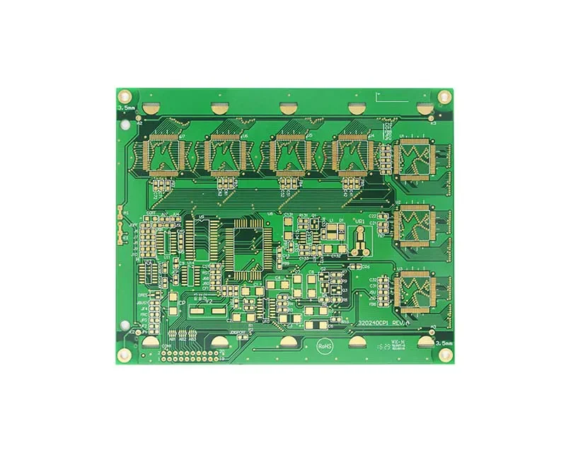
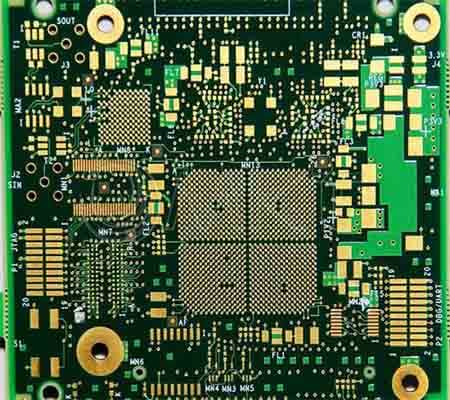
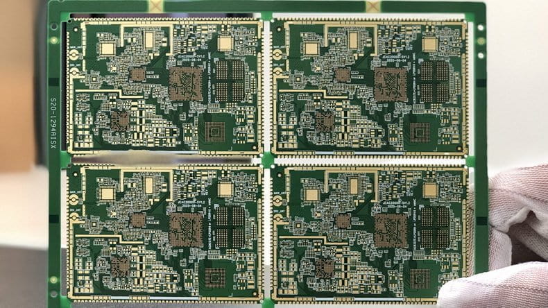
What Is a Probe Card PCB? A Probe Card PCB is a high-precision printed circuit board used in semiconductor wafer-level testing. It serves as the electrical interface between Automated Test Equipment (ATE) systems and the wafer under test. Unlike load boards used for packaged ICs, probe card PCBs are specifically designed to connect to microscopic...

Multilayer PCB – Advanced Layered Circuit Board for High-Performance Electronic Systems

What Is a Multilayer PCB? A Multilayer PCB is a printed circuit board consisting of three or more conductive copper layers laminated together with insulating dielectric materials. These layers are electrically interconnected through plated vias to create complex routing structures within a compact footprint. Compared to single-layer or double-layer boards, multilayer PCBs enable higher circuit...

Microvia PCB – Laser-Drilled HDI Technology for High-Density Interconnection

What Is a Microvia PCB A Microvia PCB is a high-density interconnect (HDI) printed circuit board that uses laser-drilled microvias to connect adjacent copper layers. Unlike traditional mechanical through-holes, microvias are extremely small and typically connect only one or two layers. Microvia technology enables higher routing density, improved electrical performance, and more compact electronic designs....

Fine Line PCB – Precision Micro-Trace Technology for High-Density Circuit Design

What Is a Fine Line PCB? A Fine Line PCB refers to a printed circuit board manufactured with extremely narrow trace widths and spacing. Compared with standard PCB designs, fine line technology enables higher routing density within limited board space. Fine line PCBs are essential for modern electronic devices where compact size, high functionality, and...

High Density PCB Design – Engineering Solutions for Complex and Compact Electronic Systems

Engineering Challenges Behind High Density PCB As electronic systems become more compact and functionally integrated, PCB designers are facing increasing layout complexity. A High Density PCB is not simply about placing more components on a board — it requires precise coordination between electrical design, stack-up engineering, manufacturability, and long-term reliability. High density PCB development focuses...

Microvia PCB – High Density Interconnect PCB for Advanced Electronic Applications

Microvia PCB for High Density Interconnect (HDI) Design As electronic products continue to shrink in size while increasing in functionality, traditional through-hole PCB structures are no longer sufficient. Microvia PCB technology enables higher routing density, improved signal integrity, and compact multilayer stackups, making it essential for modern high-performance electronics. Microvias are laser-drilled vias typically with...

Multilayer PCB – High Performance Multi Layer Printed Circuit Board for Advanced Electronics

What Is a Multilayer PCB? A Multilayer PCB is a printed circuit board composed of three or more conductive copper layers laminated together with insulating dielectric materials. Compared to single-sided or double-sided boards, Multilayer PCB technology allows significantly higher circuit density and more complex routing structures. Modern electronic systems increasingly require compact size, high speed...

Fine Pitch PCB – Precision PCB for High Density and Fine Line Applications

What Is Fine Pitch PCB? A Fine Pitch PCB refers to a printed circuit board designed with extremely small trace width and spacing to support high pin count and fine pitch components. It is commonly used in advanced electronic systems where compact design, high integration, and precise routing are essential. Fine pitch designs are typically...

HDI PCB – High Density Interconnect PCB for Advanced Electronics

What Is HDI PCB? HDI PCB (High Density Interconnect PCB) is a printed circuit board designed with higher wiring density per unit area compared to traditional multilayer PCBs. It uses advanced manufacturing technologies such as microvias, blind vias, buried vias, and fine line traces to achieve compact size and improved electrical performance. HDI PCB is...

Buried Via PCB – Advanced Multilayer PCB with Internal Interconnection Technology

What Is a Buried Via PCB? A Buried Via PCB is a multilayer printed circuit board that contains vias connecting internal layers only, without reaching the outer surface layers. Unlike through-hole vias, buried vias are completely enclosed within the board stack-up. This allows designers to: Increase routing density Optimize outer layer space Improve signal integrity...