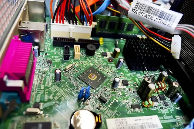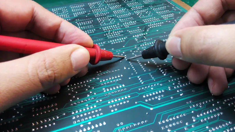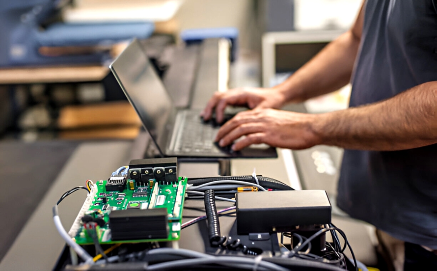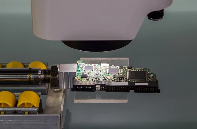
What Is a Logic Test PCB? A Logic Test PCB is a specialized printed circuit board used for functional testing and digital logic verification. It is designed to validate logic timing, signal levels, and functional behavior of ICs, modules, and electronic assemblies before mass production. Logic Test PCBs are widely used in semiconductor ATE systems,...